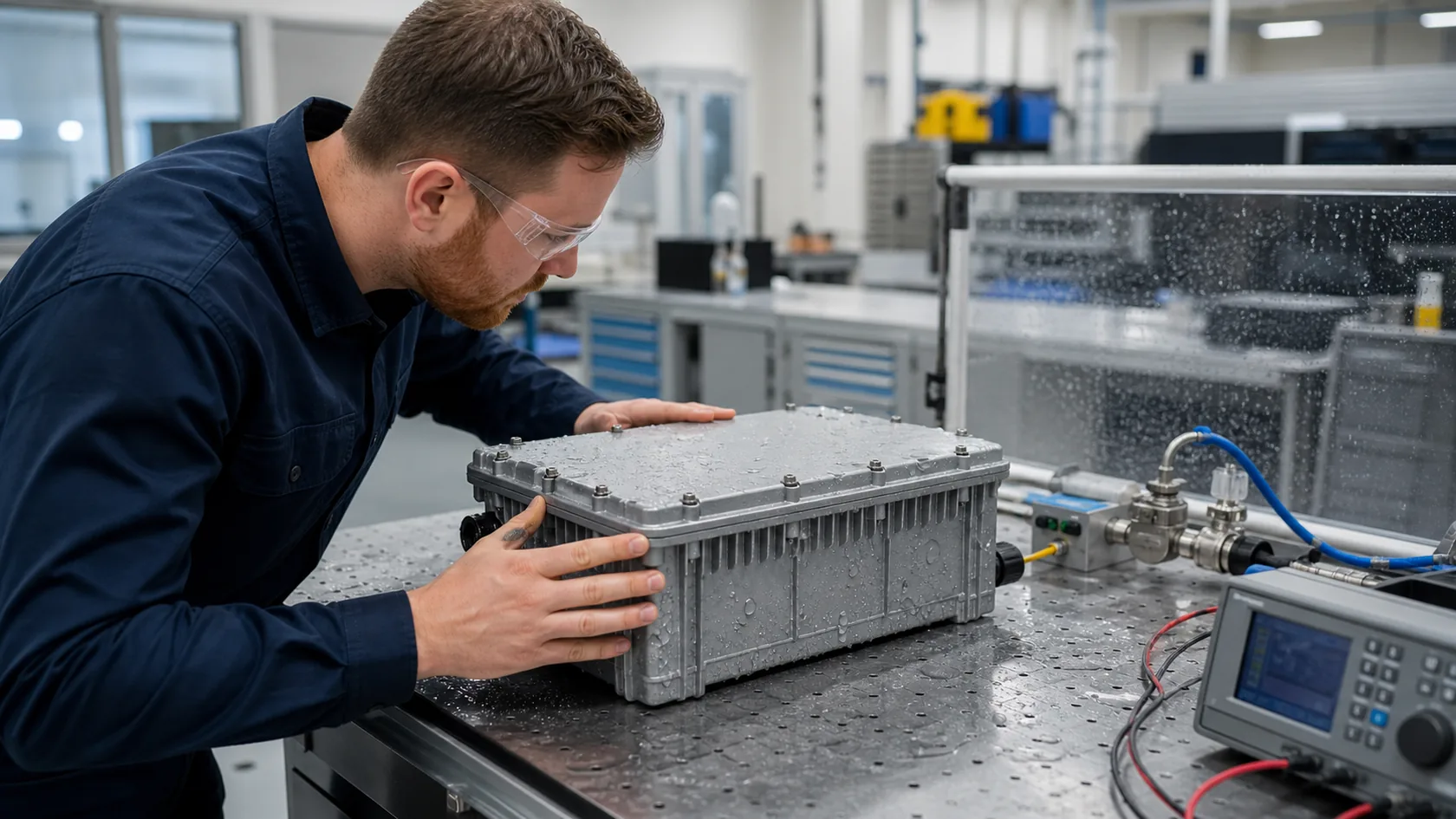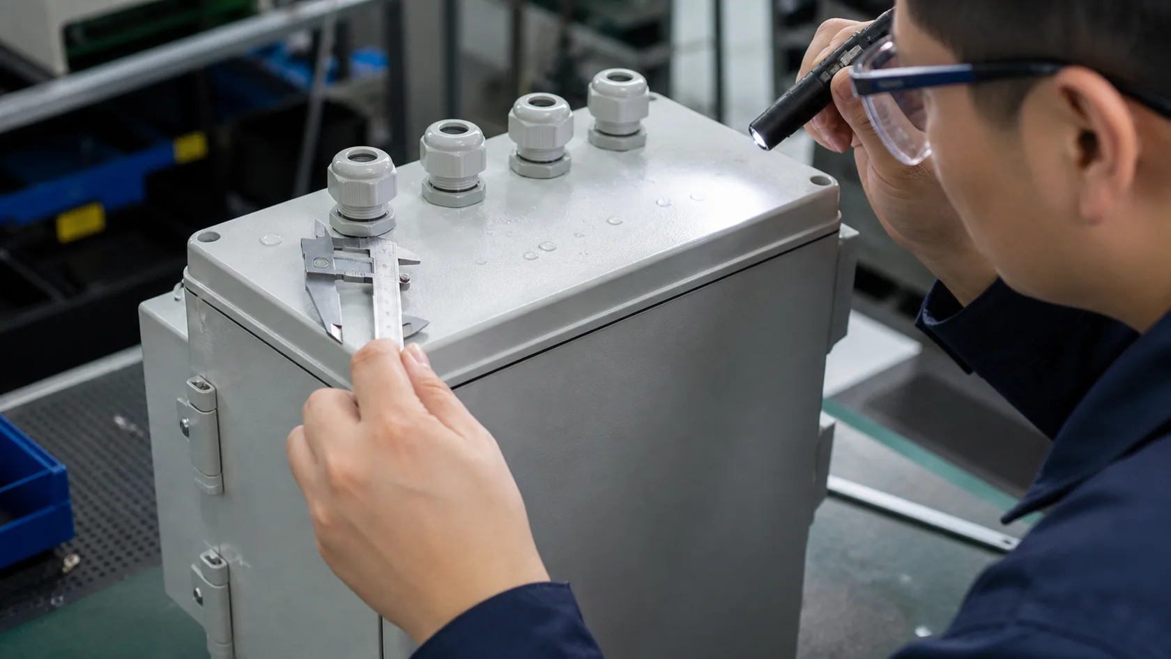
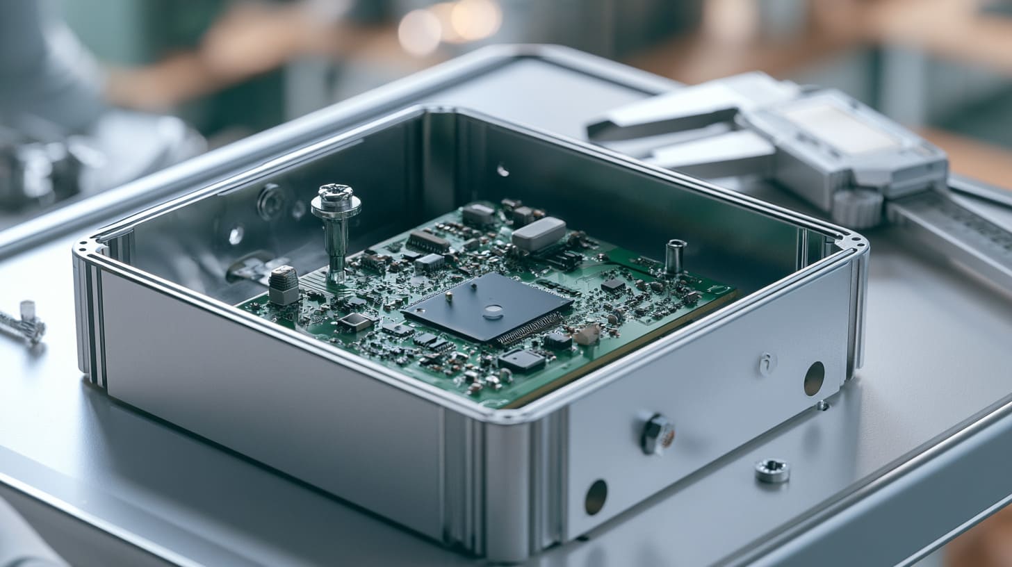
A PCB alignment problem has a funny way of blaming the wrong person.
The buyer opens the sample box. The enclosure looks fine. The PCB looks fine. Then someone tries to install the board inside the housing. One screw does not enter smoothly. The USB port sits a little too low. The RJ45 opening looks slightly off. The first reaction is often simple:
“The factory made it wrong.”
I understand this reaction. If the part does not assemble well, the factory is the easiest place to blame. But after handling many custom aluminum enclosure projects, I have learned one thing. Many PCB alignment problems do not really start on the production floor. They start much earlier, inside the drawing.
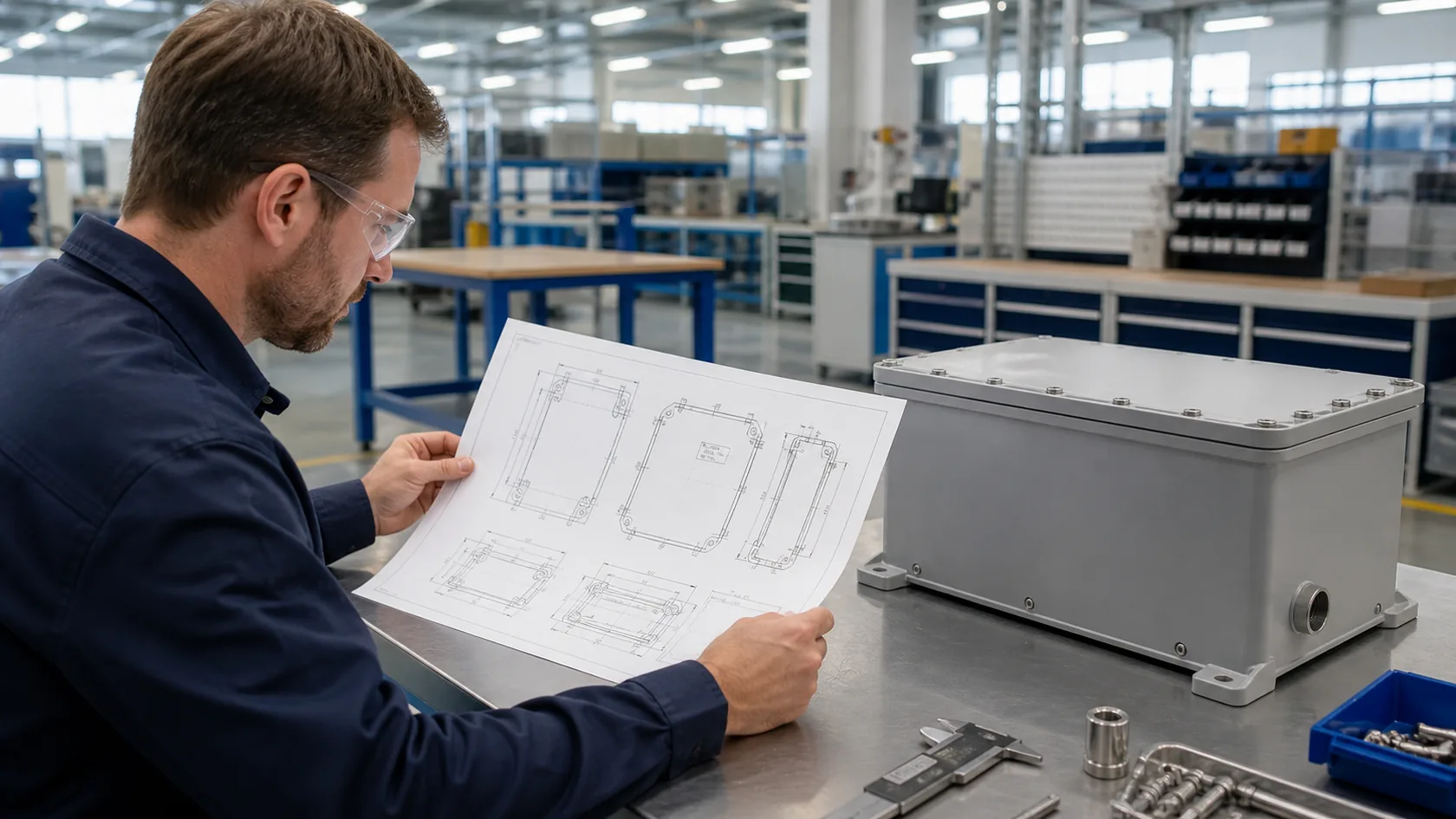
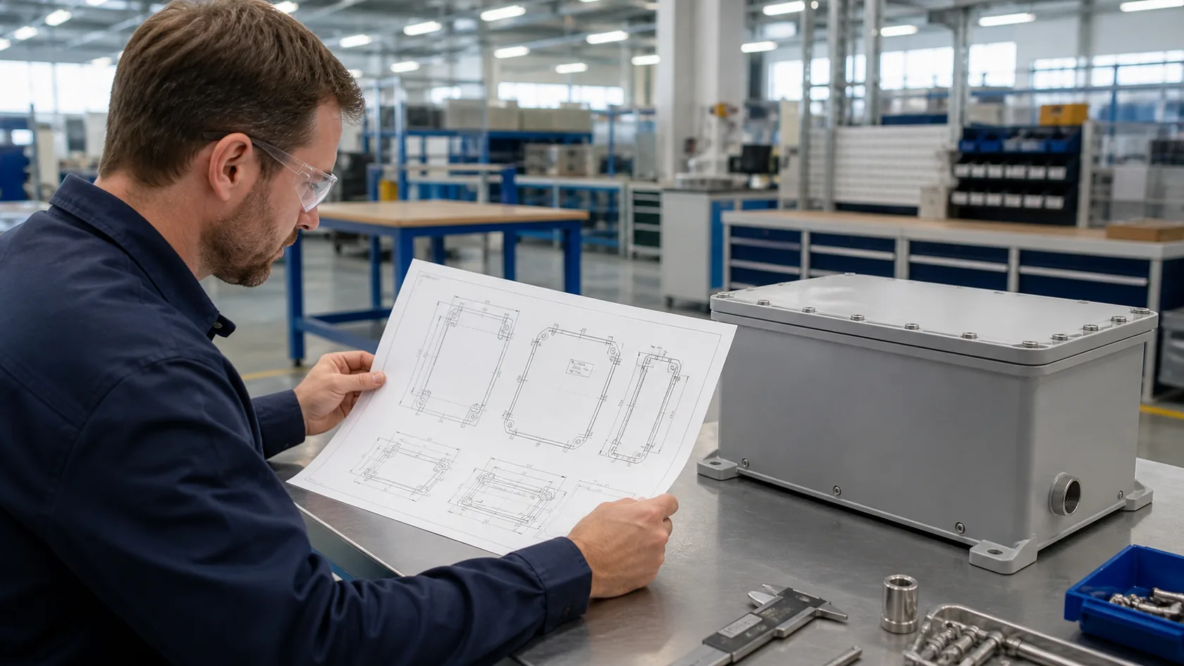
A drawing is not only a file for quotation. It is not only a document for the engineer. For custom enclosures, the drawing is the first manufacturing decision. It tells the factory what matters. It tells the CNC operator where to cut. It tells the QC team what to inspect. It tells the assembly team how the PCB should sit inside the box.
If the drawing is clear, the factory has a better chance to make a reliable enclosure. If the drawing is unclear, even a skilled factory can make a part that looks correct but fails in assembly.
This is why I slow down when I receive a PCB-related enclosure drawing. I do not only look at the outside size. I do not only look at the material and surface finish. I also look at how the PCB is controlled inside the enclosure.
Small details decide the final feeling of the product.
A 0.5 mm shift may not sound serious on paper. But when a customer sees a USB-C port not centered in the opening, it feels cheap. When a screw cannot enter a standoff, the project loses time. When the PCB touches a rib or cover, the design needs another revision.
So in this article, I want to explain why PCB alignment problems usually start with the drawing, not the factory. I will also share how I usually check these risks before production, especially in custom aluminum enclosure projects.
Why PCB Alignment Problems Often Start Before Production
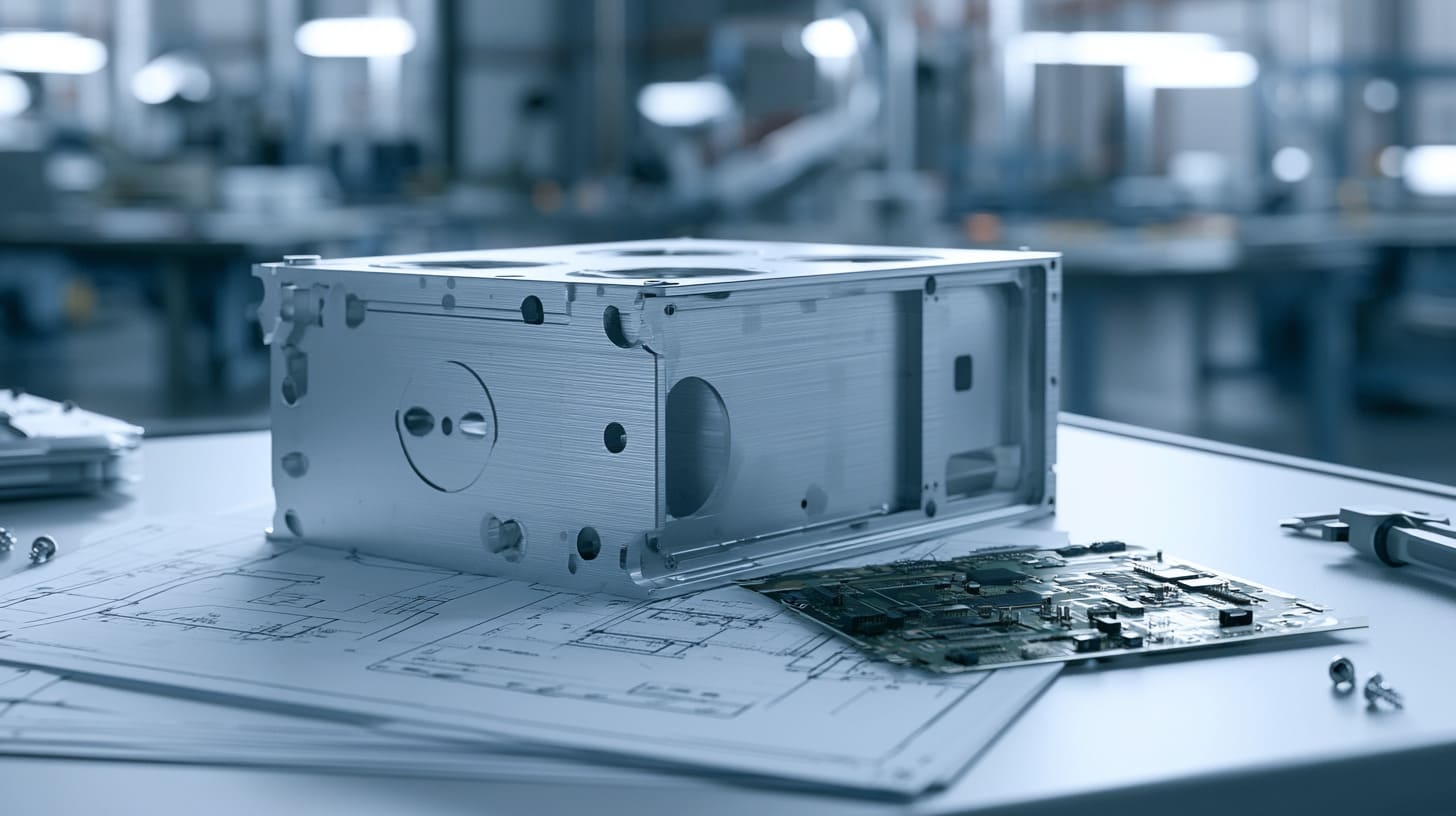
PCB alignment problems often look like assembly problems. But many of them are born before any aluminum is cut.
I have seen drawings where the enclosure size was clear, the material was clear, and the surface finish was clear. But the PCB location was almost “assumed.” The mounting holes were shown, but the reference was weak. The connector openings were drawn, but the centerline was not clear. The standoff positions were there, but nobody checked the real component space around them.
That kind of drawing looks complete at first glance. But it is not complete for manufacturing.
The drawing controls how the factory understands the product
A factory does not read a drawing like a designer reads an idea. A factory reads a drawing as a set of instructions.
If the drawing says the hole is here, the factory makes the hole there. If the drawing does not say which dimension is critical, the factory may treat all dimensions in the same way. If the drawing does not define how the PCB sits inside the enclosure, the factory may not know which feature should control the assembly.
For a custom enclosure, several features must work together:
| Feature | Why it affects PCB alignment |
|---|---|
| PCB outline | Decides whether the board can enter the housing smoothly |
| Mounting holes | Decide whether screws can lock the PCB correctly |
| Standoffs or bosses | Decide PCB height and support position |
| Connector cutouts | Decide whether ports match the enclosure panel |
| Internal ribs | May block PCB edges or components |
| Cover or sliding lid | May hit tall components |
| Surface finish | May change hole size or mating clearance |
If these features are not connected clearly in the drawing, the factory may make each feature “right” by itself. But the full assembly may still be wrong.
This is where I become careful. A drawing can look clean, but I judge it by one question: can a worker use this drawing to understand how the PCB should live inside the enclosure?
A “correct” part can still create a wrong assembly
This is a hard point for many buyers to accept.
Sometimes the enclosure passes inspection. The PCB also passes inspection. Both suppliers say their parts are within tolerance. But during assembly, the screw hole is slightly off. The connector does not sit in the center. The PCB edge touches the housing.
So who is wrong?
Maybe nobody is fully wrong. But the drawing did not protect the assembly.
For example, let us say the PCB mounting hole pattern has a small tolerance. The CNC machining on the enclosure also has a small tolerance. The extrusion body has a small variation. The powder coating adds another small change. Each one looks acceptable alone.
But when all these small movements go in the same direction, the final PCB position shifts.
| Part | Small variation that may happen |
|---|---|
| PCB | Hole drilling shift |
| Enclosure | Machining position shift |
| Standoff | Boss position or height variation |
| Surface finish | Coating build-up around holes |
| Screw | Slight clearance or angle issue |
| Assembly | Worker pushes PCB from one side |
One small movement is easy to forgive. Several small movements together become a real problem.
Why buyers often notice the problem too late
Most PCB alignment problems are not easy to see during quotation. They appear during prototype assembly.
That is why they hurt.
At quotation stage, everyone talks about price, lead time, material, color, and MOQ. But at prototype stage, people suddenly notice the hidden mechanical details. The board does not drop in smoothly. The panel cutout needs adjustment. The standoff height is not right. The screw does not align.
Then the project slows down.
The cost may include:
| Problem found during prototype | Possible result |
|---|---|
| Screw holes do not align | CNC rework or drawing revision |
| Connector is off-center | Panel cutout change |
| PCB touches internal rib | Enclosure structure change |
| Cover hits component | Height adjustment or new profile |
| Standoff is too close to component | Boss relocation |
| Coating blocks hole | Masking or hole rework |
The painful part is not only the money. It is the lost time.
For Davide-type customers, the product launch schedule matters. For John-type ODM customers, the prototype may be part of a bigger project. A small enclosure issue can delay the whole product test.
I once checked a sample where the enclosure was beautifully anodized. The finish was clean. The machining looked good. But the PCB could not sit flat because one internal support was too close to a connector leg. Nobody had checked the 3D assembly before making the sample. The part looked nice. But it was not usable.
That is the kind of mistake I try to prevent before production.
The next place I usually look is the datum. It is not exciting. It is not beautiful. But it decides where everything starts.
How Missing Datum References Create PCB Position Errors
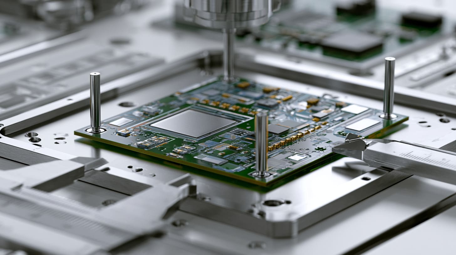
A datum sounds like a small technical word. But in real enclosure work, it is often the root of the problem.
The datum tells the factory where to measure from. It gives the drawing a “home position.” Without it, holes and cutouts may look correct in different small areas, but the full product may not align as one system.
Why datum choice matters more than many buyers expect
In a PCB enclosure, the mounting hole position should not be dimensioned randomly from different edges.
For example, one hole is measured from the left wall. Another hole is measured from the right wall. One connector cutout is measured from the outside panel. Another feature is measured from a bend line or profile edge. This looks harmless. But it can create different reference points inside one product.
When the factory manufactures the enclosure, each reference may carry its own tolerance. The result can be a small shift between the PCB and the enclosure.
A better drawing uses a clear reference logic.
| Drawing method | Risk level | Comment |
|---|---|---|
| Every hole measured from different edges | High | Easy to create accumulated error |
| Connector cutouts measured separately from PCB holes | High | Ports may not match board position |
| One main datum controls PCB hole pattern | Low | Easier to inspect and assemble |
| PCB and enclosure use matching reference | Low | Better for 3D checking and production |
My own rule is simple: if I cannot quickly see what controls the PCB position, I treat the drawing as risky, even if the dimensions look complete.
The risk of using enclosure edges as loose references
Many buyers use enclosure edges as references. This is normal. But it can be dangerous when the edge is not the best functional reference.
For example, extruded aluminum enclosures may have profile tolerance. Sheet metal enclosures may have bend variation. Die-cast housings may have shrinkage and draft angles. Plastic enclosures may have molding variation.
If the PCB position depends on a loose edge, the board may move with that edge.
This is very common with extruded aluminum cases. The outer profile may be controlled by extrusion tolerance. The inner slot or rail may be more important for PCB location. If the drawing only uses the outside wall as the main reference, the real board position may not match the connector opening as expected.
Here is a simple way to look at it:
| Reference choice | When it may be risky | Better thinking |
|---|---|---|
| Outside wall | When inner PCB rail controls the board | Reference the rail or define relation clearly |
| Front panel edge | When connector is PCB-mounted | Reference connector centerline from PCB datum |
| Cover edge | When cover has loose fit | Do not use it to control PCB location |
| Bend edge | When sheet metal bend tolerance is large | Use machined or functional features where possible |
| Random hole | When hole is not critical | Use main mounting pattern as a system |
A weak reference is like giving someone a street name but no house number. They may arrive nearby, but not exactly where you need them.
Better practice: control the PCB hole pattern as one system
PCB mounting holes should be treated as one system. They should not feel like four lonely holes.
When I review a drawing, I like to see:
- One primary datum
- One secondary reference direction
- Hole-to-hole position controlled clearly
- Connector cutouts related to the PCB position
- Critical dimensions marked differently from general dimensions
- Enough clearance for real assembly
For example, if the PCB has four mounting holes, the drawing should make it clear how the full hole pattern sits inside the enclosure. It should also show how the connector centerline relates to the same system.
| Good drawing question | Why it matters |
|---|---|
| Which datum controls PCB X direction? | Prevents left-right shift |
| Which datum controls PCB Y direction? | Prevents front-back shift |
| Which surface controls PCB height? | Prevents cover or component interference |
| Are connector cutouts tied to PCB location? | Prevents visible port offset |
| Are critical holes marked? | Helps factory inspect the right features |
When this logic is missing, the factory has to guess. Good factories ask questions. Weak factories just make the part. Either way, time is lost.
And once we talk about mounting holes, we have to talk about standoffs. That is where many “small” problems become very real in the worker’s hands.
Why Mounting Holes and Standoffs Are Common Failure Points
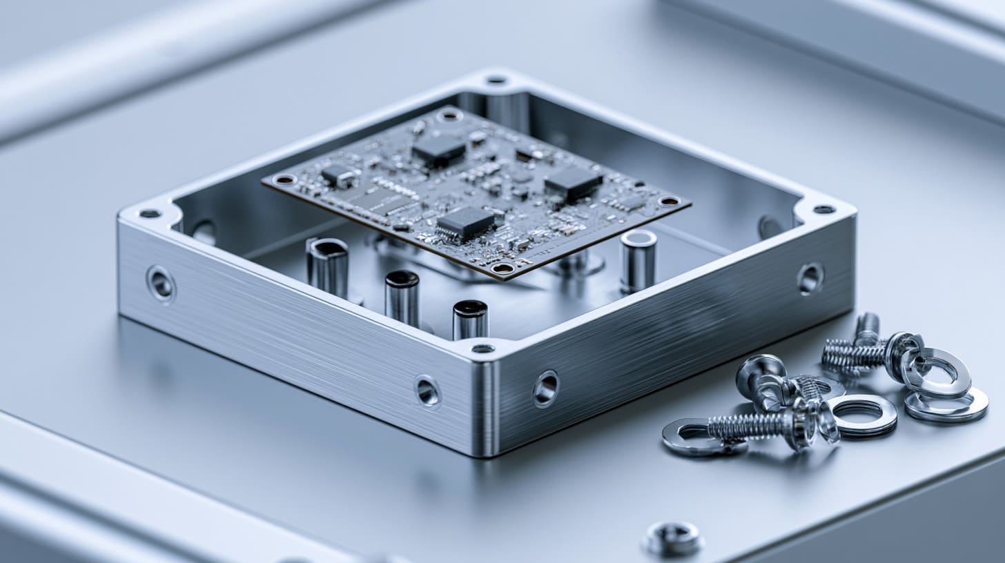
Mounting holes look simple. Standoffs look even simpler. But they create many enclosure assembly problems.
I think this happens because people often treat them as standard details. “Just add four M3 holes.” “Just use four standoffs.” “Just follow the PCB drawing.”
But in real production, there is no “just.”
Hole size is not the only issue
When buyers check PCB mounting, they often focus on screw size. M2.5. M3. M4. That is important, but it is only the starting point.
A screw hole is not only a hole. It is part of an assembly path.
You need to think about:
| Detail | Why it matters |
|---|---|
| Hole diameter | Controls screw clearance |
| Hole position | Controls PCB location |
| Standoff outer diameter | May hit nearby components |
| Standoff height | Controls PCB vertical position |
| Screw head size | Needs enough space on PCB |
| Screwdriver access | Worker must install screw easily |
| Boss strength | Must hold screw without cracking or stripping |
| Surface finish | May reduce hole clearance |
The real problem often hides around the hole, not inside the hole.
For example, a PCB hole may fit an M3 screw. But if the screw head is too close to a tall component, the worker cannot install it well. Or the standoff outer diameter may touch a solder joint. Or the hole is correct, but the standoff height makes the connector sit too low in the front panel.
In my work, I do not judge a mounting hole only by its diameter; I check whether a human hand can actually assemble the screw without fighting the product.
Standoff placement must match PCB reality
A standoff is not just a support point. It is a small tower inside the enclosure. If it is in the wrong place, it can block parts, press the PCB, or create stress.
The PCB drawing may show the mounting holes, but it may not show enough component detail. This is why a PCB STEP file is so helpful. It shows component height and space.
A standoff should avoid:
- Tall components
- Solder joints
- Connector legs
- Antenna areas
- Heat-sensitive parts
- Test points
- Cable paths
- Grounding springs
- Internal ribs
Sometimes the hole position is correct, but the standoff body is too large. This happens often when the enclosure supplier uses a standard boss size but the PCB has tight component placement.
| Standoff issue | What may happen |
|---|---|
| Boss too wide | Touches component or solder area |
| Boss too tall | PCB sits too high |
| Boss too short | Connector sits too low |
| Boss too close to wall | Screwdriver access is poor |
| Boss not strong enough | Thread may fail |
| Boss not flat | PCB may bend after tightening |
A PCB should sit naturally. It should not need force. It should not bend after screws are tightened. If the worker needs to press one corner down to catch the screw, something is already wrong.
When tight mounting holes make assembly worse
Many engineers like tight holes because tight holes look precise.
I understand that feeling. A tight tolerance feels professional. A close fit feels controlled. But in mass production, too tight can become a problem.
For PCB mounting, slight clearance often makes assembly smoother. This does not mean loose or careless. It means realistic.
| Hole design | Possible result |
|---|---|
| Very tight clearance | Hard to assemble if tolerance shifts |
| Moderate clearance | Easier assembly and lower rework risk |
| Oversized clearance | PCB may move too much |
| Slot on one side | Can absorb tolerance in one direction |
| Fixed hole + slotted hole | Can control position but allow assembly relief |
A smart design may use one fixed reference hole and one or more clearance holes or slots. This allows the PCB to locate correctly but still absorb small manufacturing variation.
This is not a shortcut. It is practical engineering.
I have seen projects where the buyer asked for very tight mounting tolerance, but the product did not need it. The result was higher CNC cost and harder assembly. After discussion, we adjusted the clearance slightly. The board still sat correctly. The assembly became easier. The cost also became more reasonable.
That is the kind of trade-off I like. Not perfect on paper. Better in real hands.
Mounting holes decide whether the PCB can sit inside the enclosure. But connectors decide how the customer sees the product from outside.
How Connector Cutouts Create Visible Alignment Problems
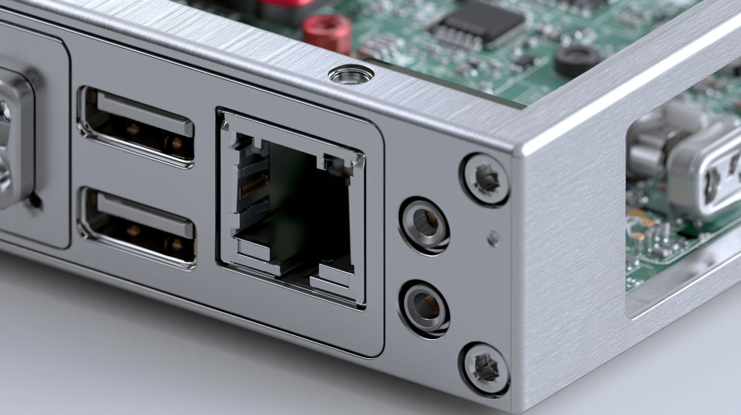
Connector alignment is cruel.
A mounting hole hidden inside the enclosure may be slightly off and nobody sees it after assembly. But a USB port, RJ45 port, HDMI port, SMA connector, or DC jack is visible from the outside. If it is not centered, the whole product looks less professional.
Even when the function is still okay, the feeling is wrong.
Connectors expose small drawing errors quickly
Connectors are easy to judge by eye. A customer does not need a caliper to notice a crooked port.
For OEM products, this matters a lot. The enclosure is part of the brand. If the front panel looks rough, the buyer may think the whole product is poorly made.
Common connector alignment problems include:
| Connector issue | How it looks or feels |
|---|---|
| USB port sits too low | Product looks cheap |
| RJ45 opening is too large | Gap looks rough |
| HDMI opening is shifted | Cable may rub the edge |
| SMA hole is not centered | Nut may not sit cleanly |
| DC jack is too close to wall | Plug may not enter smoothly |
| Terminal block opening is too tight | Wire access becomes difficult |
The small problem becomes public. Everyone can see it.
From my side, I always treat visible connector openings as cosmetic and functional features at the same time, because customers judge them with their eyes before they test them with cables.
PCB-mounted connectors need enclosure coordination
Many connector problems happen because the enclosure drawing and PCB drawing are not checked together.
A PCB-mounted connector has a fixed position on the board. But the enclosure also has wall thickness, panel thickness, cover position, gasket position, and machining tolerance. If these details are not checked, the opening may not match the real connector location.
For example, a USB connector may be drawn from the PCB origin. But the enclosure panel cutout may be drawn from the outside edge. If the PCB location inside the enclosure shifts slightly, the USB opening shifts visually.
The drawing should define:
- Connector centerline
- Cutout width and height
- Cutout corner radius
- Distance from PCB datum
- Distance from enclosure datum
- Panel thickness
- Connector protrusion depth
- Cable insertion clearance
- Surface finish effect
Here is a simple table I often use in my mind:
| Connector detail | Question I ask |
|---|---|
| Centerline | Is it linked to the PCB position? |
| Cutout size | Is there enough clearance for cable insertion? |
| Wall thickness | Will the connector sit too deep? |
| Radius | Can the CNC tool make this shape? |
| Surface finish | Will coating make the opening smaller? |
| Assembly direction | Can the PCB slide into place with connector installed? |
This is especially important for extruded aluminum enclosures with end panels. The PCB may slide into internal slots, and the connector cutouts are usually on the front or rear panel. If the PCB slot, panel, and connector are not checked together, misalignment is easy.
Cosmetic alignment and functional alignment are different
A connector can function but still look wrong.
This is a point many factories overlook. They may test whether the cable plugs in. If it plugs in, they think the part is acceptable. But the buyer may look at the front panel and feel unhappy.
For a consumer-facing or branded product, visual alignment matters. For industrial products, it also matters, but in a different way. A poorly aligned port may make the customer question the control of the whole supplier.
| Alignment type | Main concern |
|---|---|
| Functional alignment | Cable can insert and work |
| Cosmetic alignment | Port looks centered and clean |
| Service alignment | Technician can access it easily |
| Durability alignment | Cable does not rub sharp edges |
| Brand alignment | Product looks professional |
Sometimes we need to enlarge the cutout slightly. Sometimes we need to move the PCB. Sometimes we need to adjust the standoff height. Sometimes we need to change the connector model.
The mistake is assuming there is only one answer.
A connector opening is a small window. Through that window, the customer judges the whole enclosure.
After connector cutouts, the next hidden trouble is tolerance. It is quiet on paper. But it can become loud in assembly.
How Tolerance Stack-Up Turns Small Errors Into Assembly Failure
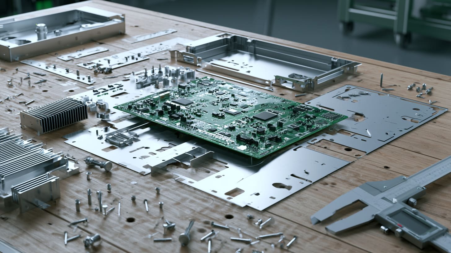
Tolerance stack-up is one of those topics that sounds boring until it costs money.
A buyer may say, “Only 0.1 mm difference should not matter.” Sometimes that is true. But sometimes several small differences move in the same direction. Then the PCB no longer fits well.
Each part may be within tolerance
In a custom enclosure project, many parts carry tolerance:
- PCB outline tolerance
- PCB drilling tolerance
- CNC machining tolerance
- Extrusion tolerance
- Sheet metal bending tolerance
- Die casting tolerance
- Plastic molding tolerance
- Surface finishing thickness
- Screw tolerance
- Standoff tolerance
- Assembly handling tolerance
Each supplier may say, “My part is within tolerance.” And they may be right.
But the product does not care about supplier excuses. The product only cares whether everything fits together.
This is why I do not only ask whether one part can meet tolerance; I ask how the tolerance moves when the PCB, enclosure, screw, finish, and worker all meet at the same moment.
The real problem is the combined movement
Let us use a simple example.
A PCB hole moves 0.10 mm. The enclosure boss moves 0.10 mm. The CNC cutout moves 0.10 mm. The extrusion profile has 0.15 mm variation. The coating adds a small thickness around the opening.
Each number looks small. But together, the final result may be visible.
| Source of variation | Example movement |
|---|---|
| PCB drilling | 0.10 mm |
| Enclosure CNC machining | 0.10 mm |
| Extrusion profile | 0.15 mm |
| Surface finish | 0.05 mm |
| Assembly shift | 0.10 mm |
| Total possible shift | 0.50 mm |
A 0.50 mm shift can matter. It may make a connector look off-center. It may make a screw hard to install. It may make the PCB rub against the enclosure wall.
This is why I often tell customers: one small tolerance is not scary. A group of small tolerances without a plan is scary.
Why drawings need assembly-based tolerance thinking
Many drawings focus on part tolerance. But assembly problems need assembly tolerance thinking.
The question is not only:
“Can the factory hold ±0.05 mm?”
The better question is:
“Does this feature really need ±0.05 mm, and what happens if all related parts move to the worst side?”
Tight tolerance is not always better. It can increase cost and slow production. Loose tolerance is not always bad. It can be safe if the feature is not critical.
| Feature | Suggested thinking |
|---|---|
| Connector centerline | Usually critical |
| PCB mounting hole pattern | Critical for assembly |
| Outside cosmetic length | Depends on product |
| Internal clearance | Needs enough safety margin |
| Screw clearance hole | Should not be too tight |
| Decorative surface | More about appearance than fit |
A good drawing should separate critical dimensions from general dimensions. If every dimension is marked tight, the factory does not know what really matters. The cost goes up. The risk may still remain.
I like drawings that tell me the designer’s real intention. Which feature controls function? Which feature controls appearance? Which feature can allow more tolerance? This makes manufacturing smarter.
But tolerance tables still cannot show everything. Some problems only appear when we see the parts in 3D.
Why 2D Drawings Alone Are Often Not Enough
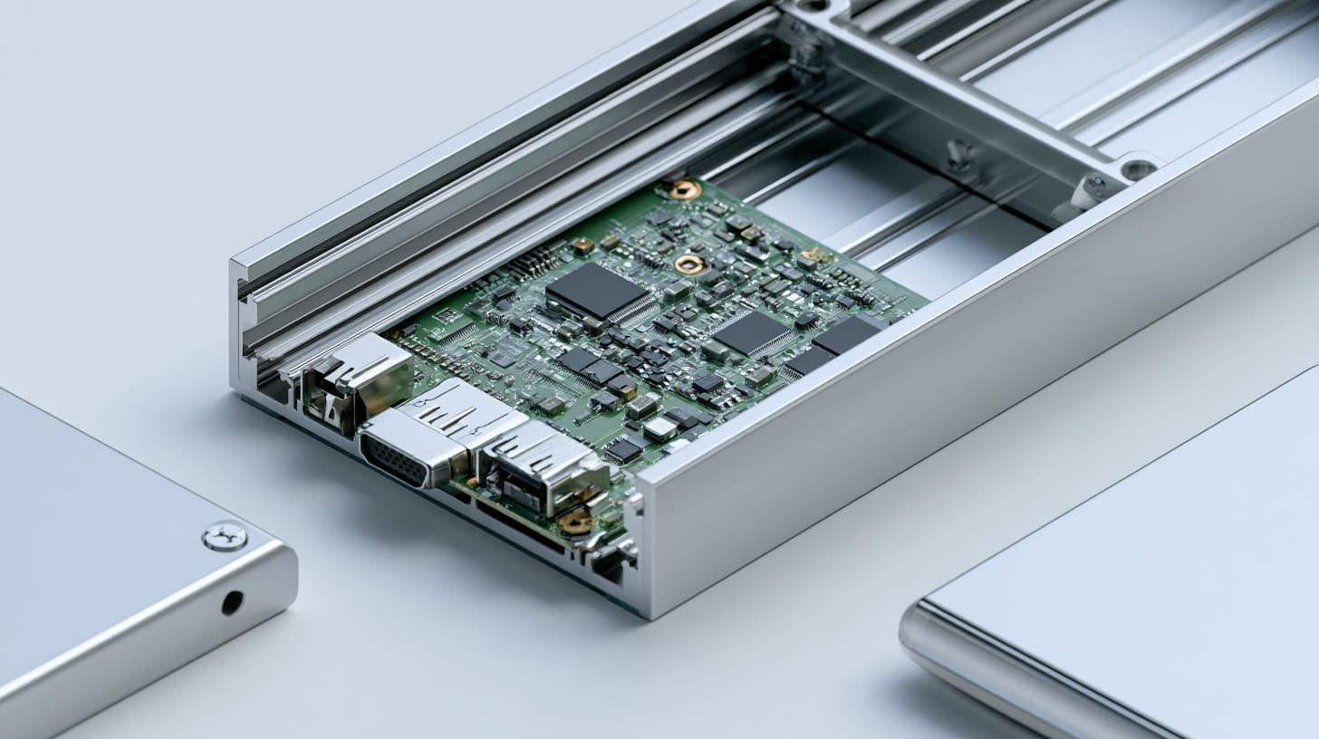
A 2D drawing is useful. I still need it. The factory still needs it. QC still needs it.
But for PCB alignment, 2D drawings are often not enough.
A 2D drawing can show hole positions. It can show cutout sizes. It can show outside dimensions. But it may not show the real relationship between the PCB, connectors, components, ribs, cover, screws, and assembly path.
2D drawings can miss interference problems
Some problems are not easy to see in 2D.
A component may be too tall. A rib may block the PCB edge. A connector may sit too deep behind the panel. A sliding cover may hit a capacitor. A gasket may compress into a space that looked empty.
The 2D drawing may look correct, but the product may still fail.
| Hidden issue | Why 2D may miss it |
|---|---|
| Component height | Top view may not show it clearly |
| Internal rib interference | Section view may be missing |
| Connector depth | Front view may not show full body |
| Cover sliding path | Static drawing may miss assembly movement |
| Cable bending space | Cable path may not be shown |
| Gasket compression | Final compressed shape may be unclear |
I become especially careful when the customer only sends a flat drawing but the enclosure has many internal features. A flat drawing can tell me where holes are, but it cannot always tell me whether the product has room to breathe.
STEP files reduce misunderstanding
A PCB STEP file and an enclosure STEP file make the discussion much clearer.
With 3D files, we can check:
- PCB position inside the enclosure
- Component height
- Standoff location
- Screw access
- Connector cutout match
- Internal wall clearance
- Cover fit
- Heat sink position
- Cable path
- Assembly direction
This does not mean 3D checking replaces 2D drawings. It does not. The 2D drawing still controls dimensions and tolerance. But the STEP file helps everyone see the same product.
For custom aluminum enclosures, this is very important. Aluminum parts are often more expensive to rework than plastic parts. If the enclosure needs anodizing or powder coating, rework may also damage the finish.
3D checking should happen before quotation is finalized
Some buyers send STEP files only after placing the order. I think this is risky.
If the factory checks the 3D file after order confirmation, new problems may appear. Then the price changes. The lead time changes. The customer becomes unhappy. The supplier also feels pressure.
It is better to check early.
| Checking time | Result |
|---|---|
| Before quotation | Risk is found early, cost is clearer |
| After quotation but before order | Some adjustment is still possible |
| After order confirmation | Price and schedule may be affected |
| After prototype | Rework or redesign may be needed |
| After mass production | Serious cost and trust problem |
For me, a STEP file is not just an engineering file. It is a way to reduce arguments later.
When both sides see the same 3D assembly, the discussion becomes more honest. We can say, “This connector may hit the panel,” or “This standoff is too close to the component,” before money and time are wasted.
But even when the 3D design is good, surface finishing can still change the final fit. That is another detail many drawings forget.
How Surface Finishing Can Shift Final Assembly Fit
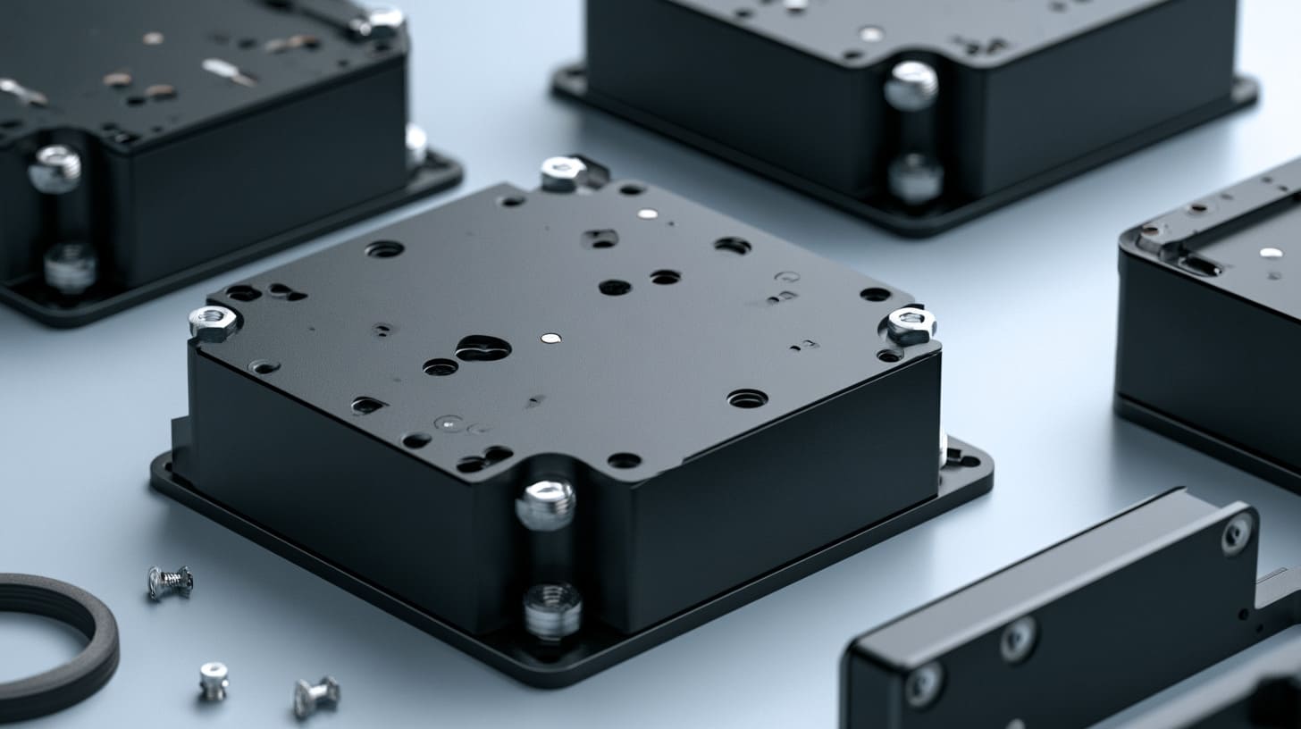
Surface finishing looks like the last step. But it should be considered much earlier.
Powder coating, anodizing, painting, plating, and other finishes all affect the final part in different ways. Some effects are small. Some are easy to control. But if the drawing ignores them, the assembly may suffer.
Coating thickness changes real dimensions
Powder coating adds thickness. Anodizing changes the surface in another way. Painting and plating also affect edges, holes, slots, and contact surfaces.
This matters for PCB alignment because the PCB depends on real space, not raw machining space.
| Surface finish | Possible effect on PCB assembly |
|---|---|
| Powder coating | May reduce hole or slot clearance |
| Anodizing | May affect grounding contact |
| Painting | May build up near edges |
| Plating | May change tight mating areas |
| Sandblasting before finish | May slightly affect surface feel and fit |
A hole that fits before coating may become tight after coating. A sliding cover that moves smoothly before coating may feel stuck after coating. A grounding point may lose contact if it is fully coated.
Before I accept a tight internal fit, I want to know whether the dimension is for raw machining or final finished condition, because that small note can decide whether the sample feels smooth or frustrating.
Masking areas may be needed
Masking means protecting some areas from coating or finish. This is often needed in functional zones.
Common masking areas include:
- Grounding contact points
- Screw holes
- PCB support surfaces
- Connector cutout edges
- Sliding surfaces
- Threaded holes
- Heat transfer surfaces
- Label or bonding areas
For example, if the enclosure needs EMI grounding, a fully powder-coated internal surface may block electrical contact. If a screw hole is heavily coated, the screw may not enter smoothly. If a heat transfer surface is coated too thick, thermal contact may become worse.
| Area | Why masking may help |
|---|---|
| Threaded hole | Keeps screw fit stable |
| Grounding pad | Keeps electrical contact |
| Heat sink contact area | Improves heat transfer |
| Sliding rail | Keeps smooth movement |
| Connector edge | Keeps cutout size stable |
| PCB support point | Keeps board height stable |
Masking adds cost and handling steps. But sometimes it is much cheaper than rework.
Why finishing should be discussed before production
Many drawings only say “black powder coating” or “clear anodized.” That is not always enough.
The drawing should tell the factory whether critical dimensions are before or after finishing. It should also say which areas need masking.
If this is not clear, the factory may machine the raw part correctly. Then after finishing, the final part becomes tight, blocked, or electrically isolated.
This is not always a factory mistake. Sometimes the drawing simply did not ask the right question.
For custom OEM enclosures, I prefer to discuss finishing together with assembly. Not after assembly. Not after the sample fails. Together.
Once finishing is clear, the buyer should also provide the right files. Without enough information, even a good supplier has to guess.
What Information Buyers Should Provide With the Drawing

A good RFQ is not only about sending a drawing and asking for price.
For PCB-related enclosure projects, the quality of the information decides the quality of the quotation. It also decides how many questions come later.
I do not expect every buyer to send perfect files. Many projects are still developing. But I do hope buyers can share the information that controls assembly risk.
PCB files and mechanical files
The more the enclosure factory understands the full product, the better it can help.
Useful files include:
| File or information | Why it helps |
|---|---|
| PCB outline drawing | Shows board size and mounting holes |
| PCB STEP file | Shows component height and connector position |
| Enclosure STEP file | Shows real internal structure |
| 2D enclosure drawing | Controls dimensions and tolerance |
| Connector datasheets | Confirms cutout and clearance needs |
| Assembly direction | Shows how the PCB enters the housing |
| Mounting screw specification | Confirms hole and boss design |
| Surface finish requirement | Helps check final fit |
| Logo or branding file | Helps plan engraving or printing area |
When I receive only the enclosure drawing, I can quote the enclosure. But I may not be able to judge the PCB risk well.
That is the difference.
Critical alignment requirements
Not every dimension is equally important.
Some connectors must be visually centered. Some holes must be very accurate. Some surfaces are only cosmetic. Some areas can allow more clearance.
Buyers should tell the factory what really matters.
| Requirement | Example |
|---|---|
| Must be visually centered | USB-C, HDMI, front LED window |
| Must be functionally accurate | Mounting holes, grounding points |
| Can allow more clearance | Cable exit slot, internal free space |
| Must be controlled after finish | Sliding rail, threaded holes |
| Cosmetic surface | Front panel, top cover, logo area |
| Hidden surface | Internal wall, bottom side |
One thing I pay attention to is the buyer’s real concern. If the customer cares about front panel appearance, I focus more on connector centering and surface finish. If the customer cares about field service, I look harder at screw access and cable clearance.
Different products need different judgment.
Real use conditions
PCB alignment is not only about the drawing. The working environment also matters.
For example:
- Vibration may loosen screws or stress the PCB.
- Outdoor use may need sealing and gasket compression.
- Heat may need thermal pads or heat sink contact.
- EMI may need grounding paths.
- IP sealing may affect connector placement.
- Service access may need more space around screws and cables.
| Use condition | Design concern |
|---|---|
| Vibration | Screw locking, PCB support, stress points |
| Outdoor use | Gasket, drainage, corrosion resistance |
| Heat generation | Thermal path, airflow, contact surface |
| EMI requirement | Grounding, coating removal, conductive contact |
| IP sealing | Connector seals, gasket compression |
| Field maintenance | Easy screw access and cable removal |
If the buyer only sends dimensions, the factory may miss the real use risk. If the buyer shares the product environment, the factory can give better suggestions.
A custom enclosure is not a box around a PCB. It is part of the product system.
That is why we also have our own review method before production at MaidaTech.
How MaidaTech Reviews PCB Alignment Risk Before Production
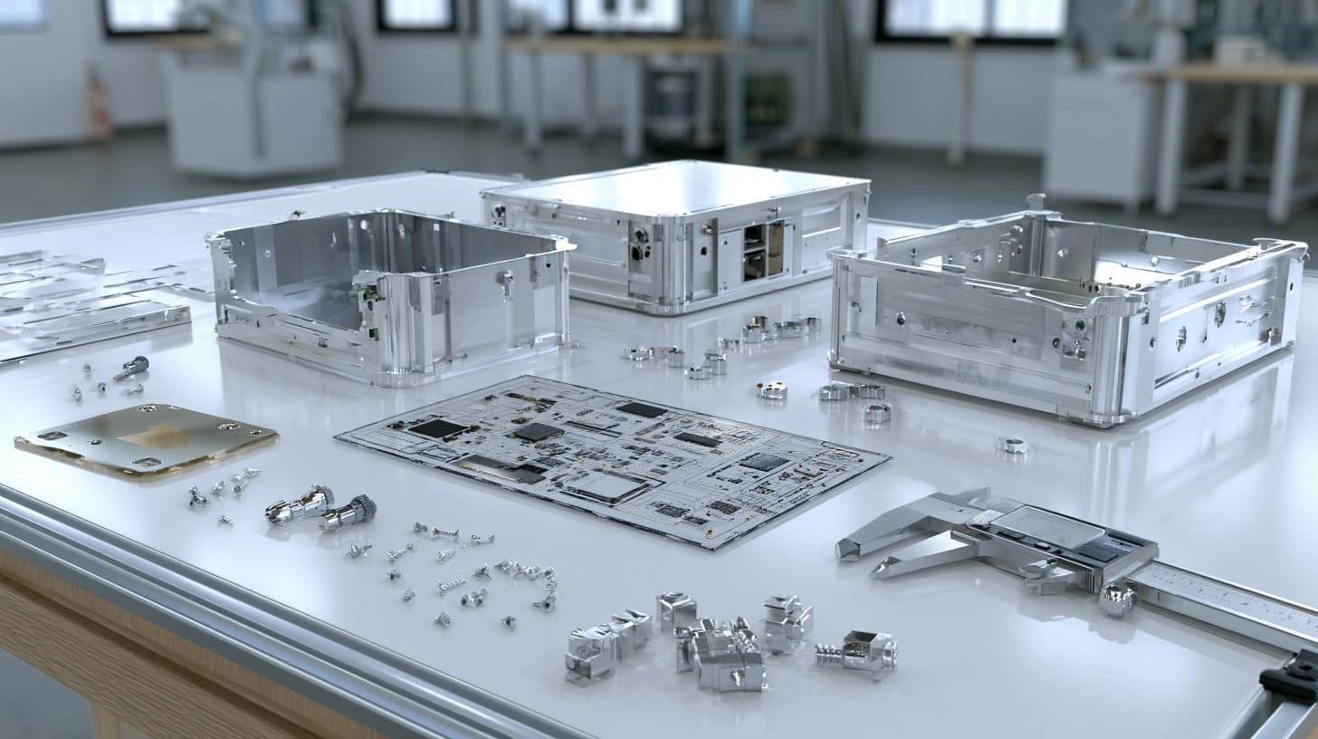
At MaidaTech, I do not want to wait until the sample is finished to discover a basic alignment problem.
Of course, not every issue can be found before prototype. That would be unrealistic. But many obvious risks can be reduced if we check the drawing properly.
First check: drawing logic
The first thing I check is not the color. It is not even the outside size.
I check the drawing logic.
I ask:
- Are the PCB mounting holes controlled from a clear datum?
- Are connector cutouts dimensioned from the same reference system?
- Are critical tolerances marked clearly?
- Are there too many dimensions from different edges?
- Is the PCB position defined, or only implied?
If the drawing logic is weak, production will become risky.
| Drawing item | What I check |
|---|---|
| Datum | Is there a clear reference? |
| Mounting holes | Are they controlled as a pattern? |
| Connector openings | Are centerlines clear? |
| Critical dimensions | Are they marked? |
| Tolerance notes | Are they realistic? |
| Finish notes | Are dimensions raw or final? |
I like to catch the logic problem before we talk too much about price, because a cheap price does not help if the first sample cannot assemble.
Second check: 3D assembly
After the drawing logic, I prefer to check the 3D assembly.
This is where the PCB STEP file becomes very useful.
We check:
- Does the PCB fit inside the enclosure?
- Do components hit the cover?
- Do connectors match the cutouts?
- Do screws have enough access?
- Are standoffs clear from components?
- Is there enough clearance for assembly?
- Does the board slide in smoothly if it uses internal slots?
- Does the gasket or cover affect space?
| 3D area | Possible risk |
|---|---|
| PCB edge | Touches inner wall or rib |
| Connector | Misaligns with cutout |
| Component height | Hits top cover |
| Standoff | Touches nearby parts |
| Screw access | Tool cannot enter straight |
| Cable path | Cable bends too sharply |
| Thermal pad | Contact area is not enough |
I do not see 3D checking as extra work. I see it as insurance.
It is much easier to move a hole in a CAD file than to explain to a customer why the sample needs rework.
Third check: manufacturing reality
A drawing can be beautiful but still difficult to manufacture.
So we also check the process.
Can CNC machining hold the requested tolerance? Is extrusion suitable? Is sheet metal bending more practical? Does die casting make sense for the volume? Will plastic molding create a better cost structure? Will anodizing or powder coating affect the final fit?
| Process | PCB alignment concern |
|---|---|
| CNC aluminum enclosure | Good precision, higher cost |
| Extruded aluminum enclosure | Good for profiles, need slot and panel control |
| Sheet metal enclosure | Bend tolerance must be considered |
| Die-cast enclosure | Tooling and draft need early planning |
| Plastic enclosure | Shrinkage and boss strength matter |
| Hybrid structure | Different parts need assembly control |
The best process is not always the most precise process. The best process is the one that matches the product function, quantity, cost target, and assembly risk.
Sometimes I suggest a customer change a sharp internal corner because the CNC tool cannot make it cheaply. Sometimes I suggest more clearance around a connector because the coating will reduce the opening. Sometimes I suggest moving a standoff because the screw access is too poor.
This is not about making the drawing easier for us. It is about making the final product easier to build.
Still, even with good review, some drawing mistakes appear again and again. They are common because they look small.
Common Drawing Mistakes That Lead to PCB Alignment Problems
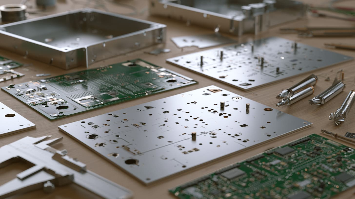
Most PCB alignment mistakes are not dramatic. They are quiet mistakes.
They hide in small dimensions. They hide in missing centerlines. They hide in “standard” holes. They hide in files that were never checked together.
Dimensioning every hole from different edges
This is one of the most common problems.
A drawing may show all hole positions, but each hole is measured from a different edge. The drawing looks full of dimensions. But the logic is weak.
This creates inconsistent reference points.
| Mistake | Why it causes risk |
|---|---|
| Hole A from left edge | Left edge has its own tolerance |
| Hole B from right edge | Right edge has another tolerance |
| Hole C from front edge | Front edge may shift after machining |
| Connector from panel edge | Not linked to PCB hole pattern |
A better method is to control the hole pattern from one main datum.
I usually become suspicious when a drawing has many dimensions but no clear priority, because too many numbers can still fail to tell the factory what actually controls the product.
Forgetting connector centerlines
Connector openings need more than rough hole size.
The centerline matters. The connector body matters. Cable access matters. The front panel thickness matters. The visual position matters.
If the drawing only shows a rectangle for a USB opening, the factory may not know how it relates to the PCB connector.
A good connector drawing should show:
- Centerline position
- Cutout size
- Corner radius
- Panel thickness
- Clearance requirement
- Related PCB datum
- Surface finish requirement
- Inspection priority
| Weak connector note | Better connector note |
|---|---|
| “USB hole here” | USB centerline from PCB datum |
| “RJ45 cutout” | RJ45 cutout size, radius, and centerline |
| “DC jack hole” | Hole diameter, nut clearance, wall thickness |
| “SMA opening” | Center hole, flat area, washer space |
A connector is not only a hole. It is an interface between the PCB and the user.
Ignoring screw clearance
Many drawings show screw thread size but forget the space needed to install the screw.
The worker needs room for fingers, screwdriver angle, screw head, washer, and sometimes thread-locking material.
If the screw is too close to a wall or component, assembly becomes slow. If the screw head touches a component, the PCB may be damaged. If the screwdriver cannot enter straight, the thread may be stripped.
| Screw detail | Why it matters |
|---|---|
| Screw head diameter | Needs space on PCB |
| Washer size | May touch components |
| Screw length | May bottom out or fail to lock |
| Tool access | Worker needs straight entry |
| Thread depth | Affects strength |
| Boss height | Controls PCB level |
These are small things. But small things decide production speed.
A design that takes 20 seconds to assemble is very different from a design that takes 2 minutes and needs careful hand adjustment.
Treating PCB files and enclosure files separately
This mistake happens when the PCB engineer and enclosure supplier work in two separate worlds.
The PCB file is correct. The enclosure file is correct. But nobody overlays them.
That is dangerous.
The PCB and enclosure should be reviewed as one assembly. The connector should match the cutout. The holes should match the standoffs. The component height should match the cover. The cable path should match the opening.
| Separate review | Assembly review |
|---|---|
| PCB checked alone | PCB checked inside enclosure |
| Enclosure checked alone | Enclosure checked with PCB |
| Connector position assumed | Connector cutout verified |
| Height risk hidden | Component clearance checked |
| Assembly path ignored | Installation direction checked |
A product is not built in separate files. It is built as one object.
Not defining critical dimensions
If every dimension looks important, no dimension is truly important.
This is another common problem.
Some drawings apply very tight tolerance everywhere. This increases cost, but it does not always reduce risk. Other drawings do not mark critical dimensions at all. This makes inspection weak.
The drawing should tell the factory where to focus.
| Dimension type | Example |
|---|---|
| Critical functional dimension | PCB mounting hole pattern |
| Critical visual dimension | Connector centerline |
| Controlled after finish | Sliding rail width |
| General dimension | Overall size with normal tolerance |
| Flexible dimension | Internal open space |
When the drawing does not define critical dimensions, QC may inspect the wrong things very carefully and miss the real problem.
That is why prevention is better than correction. A better drawing saves time before the first sample is made.
How to Prevent PCB Alignment Problems in Custom Enclosure Projects
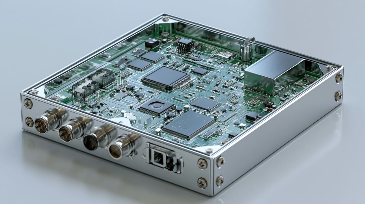
PCB alignment problems cannot be removed by hope.
They need early checking. They need clear drawings. They need realistic tolerance. They need communication between PCB design and enclosure manufacturing.
The good news is that many problems are preventable.
Lock the mechanical reference early
The first step is to decide the mechanical reference.
Where does the PCB position start? Which feature controls it? Which direction matters most? Which connector must match the panel?
If this is not decided early, the design may grow in different directions. The PCB designer may use one reference. The enclosure designer may use another. The factory may follow the drawing but still miss the design intention.
| Early decision | Why it helps |
|---|---|
| Main datum | Controls PCB location |
| PCB height | Controls connector and cover fit |
| Connector centerline | Controls front panel appearance |
| Mounting hole pattern | Controls screw assembly |
| Critical clearance | Prevents interference |
I prefer to solve the reference question before discussing small details, because if the reference is wrong, every later dimension can become a nicely measured mistake.
Review PCB and enclosure together
Do not approve the enclosure drawing without checking the PCB position.
This sounds basic, but it is often missed when the project is moving fast.
The review should include:
- PCB outline
- Mounting holes
- Standoffs
- Connector cutouts
- Component height
- Screw access
- Cable path
- Cover movement
- Gasket compression
- Surface finish effect
A simple review table can help:
| Review point | Pass question |
|---|---|
| PCB entry | Can the board enter without force? |
| Mounting holes | Do holes and standoffs match? |
| Connectors | Are ports centered and usable? |
| Height | Does the cover clear all components? |
| Screws | Can tools reach all screws? |
| Finish | Will coating affect fit? |
| Service | Can the board be removed later? |
A product should be checked the way it will be assembled, not only the way it is drawn.
Use realistic tolerance instead of blindly tight tolerance
Tolerance should match function.
A tight tolerance on the wrong feature wastes money. A loose tolerance on a critical feature creates risk.
So the better question is not, “How tight can you make it?” The better question is, “Which tolerance protects the assembly?”
| Situation | Better tolerance thinking |
|---|---|
| Connector visual position | Keep tighter control |
| Screw clearance hole | Allow practical clearance |
| Internal open space | Avoid over-controlling |
| Sliding part | Control after finishing |
| Grounding surface | Define finish and contact area |
| Cosmetic outside size | Match appearance need |
Sometimes customers think a tighter tolerance proves better quality. But in factory work, quality is not about making every number difficult. Quality is about controlling the right number.
Prototype before mass production
A prototype is not a formality. It is a real test.
The first article sample shows whether the PCB fits, whether the connector looks right, whether the screw access is good, and whether the finish affects assembly.
For custom OEM enclosures, this step is worth it.
| Prototype check | What it reveals |
|---|---|
| PCB installation | Hole and standoff alignment |
| Connector plugging | Cutout and cable clearance |
| Cover closing | Component height risk |
| Screw tightening | Boss strength and access |
| Surface finish | Final fit and appearance |
| Handling | Real assembly feeling |
Prototype review is cheaper than mass production rework. It also protects trust between buyer and supplier.
I like customers who test the prototype carefully and give clear feedback. A good sample review is not complaining. It is project control.
If we find a problem at prototype stage, we still have time to improve it. If we find it after mass production, everyone suffers.
Conclusion
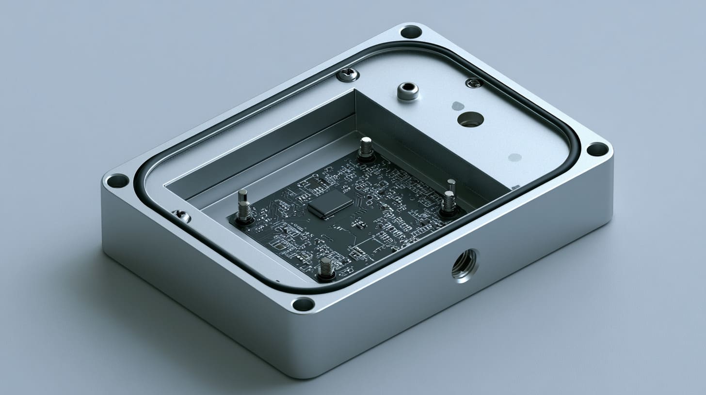
PCB alignment problems usually do not begin at the assembly bench.
They often begin when the drawing does not clearly define the PCB position, datum, mounting hole pattern, connector centerline, tolerance, surface finish effect, or 3D assembly relationship.
This is why I do not treat drawings as simple quotation files. I treat them as the first risk control tool.
I believe this because I have seen too many “factory problems” that were not only factory problems. The CNC machine followed the drawing. The worker followed the process. The QC team checked the dimensions. But the assembly still failed because the drawing did not describe how the PCB, enclosure, connector, screw, and finish should work together.
That experience changed how I review custom enclosure projects.
I now look at the drawing with a simple mindset:
Can this part be made?
Can this PCB be installed?
Can the connector look right?
Can the worker assemble it without fighting?
Can the final product still feel reliable after finishing?
These questions are not complicated. But they are practical. They help catch problems before aluminum is cut, before coating is done, and before the buyer loses time on a delayed prototype.
For product engineers, purchasing managers, and OEM buyers, my suggestion is simple. Do not send only a drawing and wait for a price. Send the PCB file, STEP file, connector information, surface finish requirement, and critical alignment notes together. The more clearly the factory understands the assembly, the fewer surprises you will face later.
At MaidaTech, we help customers make custom aluminum enclosures, plastic enclosures, sheet metal enclosures, and OEM/ODM enclosure solutions based on their real product needs. If you are working on a PCB-based enclosure and you are not sure whether the drawing is ready for production, you can send us the files for review.
A better drawing does not only make the factory’s work easier.
It protects your product.
It protects your schedule.
And sometimes, it protects you from a very expensive 0.5 mm mistake.