Skip to content
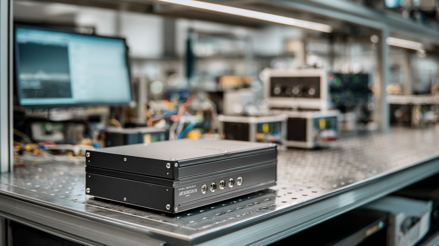
A metal enclosure can look excellent on the table and still create trouble the moment it enters an EMI test. I have seen that gap often enough that I no longer trust surface finish choices just because they look neat on a drawing. Full anodizing is one of those choices. It feels safe. It sounds professional. It gives buyers a clean story about corrosion resistance, scratch resistance, and product appearance. That is exactly why people approve it too quickly.
I understand the attraction. A fully anodized aluminum enclosure usually looks more complete than a raw one. It feels more finished in the hand. It also gives the product a more stable, premium image, which matters a lot when a buyer wants to impress customers or support a strong brand. But EMI does not care about appearance. EMI only cares about whether current can move across the enclosure surface in a stable way.
That is where the real conflict starts.
The same anodized layer that helps protect aluminum can also work like a barrier. It can interrupt the conductive path at seams, around screws, under contact points, and across areas where shielding depends on real electrical continuity. That is why I do not treat full anodizing as a neutral finishing choice on EMI-sensitive enclosure projects. I treat it as a decision that needs to be questioned.
One detail I weigh very early is this: if the enclosure needs the metal shell itself to help with shielding, I become very cautious the moment someone says, “Let’s anodize everything.”
I learned this the hard way on projects where the enclosure looked right, the machining looked right, and the assembly looked right, but the test result still pointed back to the enclosure body. That kind of failure is frustrating because it hides behind a finish that everyone thought was helping. In reality, it was helping in one direction and hurting in another.
So this article is not about saying anodizing is bad. I do not think that is true. I think the real question is much more practical: when should I stop and say no to full anodizing on an EMI-sensitive enclosure?
That is where the discussion gets more useful, because before I can judge when full anodizing becomes risky, I first need to look at what it actually does to aluminum.
What Does Full Anodizing Actually Do to Aluminum?
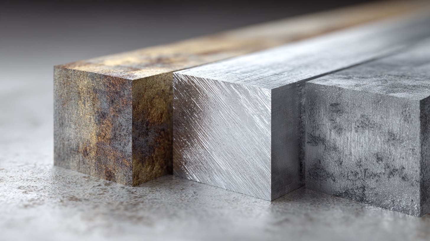
Full anodizing changes aluminum in a way that is both helpful and risky. That is why this topic creates so much confusion. One team member looks at the finish and sees better durability. Another looks at the same finish and sees a broken conductive path. In a way, both are right.
I think many problems start because people use the word anodizing too loosely. They treat it like a color or a cosmetic treatment. It is much more than that. It changes the surface condition of the metal, and that matters a lot in EMI work.
Formation of the Oxide Layer
Anodizing builds an oxide layer on the aluminum surface. This oxide layer is not just dirt or natural aging. It is a controlled electrochemical layer. It is harder than raw aluminum, and it gives better corrosion resistance. That is why it is widely used on industrial housings, consumer enclosures, and branded metal parts.
But there is a catch. Aluminum oxide is not conductive like base aluminum.
That means when I approve anodizing, I am not only approving a visual finish. I am also approving a surface layer that changes how electricity behaves at the outer skin of the enclosure.
Here is a simple way I look at it:
| Surface Condition | Appearance | Corrosion Resistance | Surface Conductivity |
|---|---|---|---|
| Raw aluminum | Plain | Low to medium | High |
| Full anodized aluminum | Clean and premium | High | Low |
| Selectively masked anodized aluminum | Mixed | High in most areas | Controlled at contact areas |
A lot of buyers only compare the first two columns. EMI design forces me to care about the fourth one.
Electrical Impact on Surface Conductivity
This is the part that people skip too often.
EMI shielding performance depends a lot on conductive continuity. If the outer shell needs to carry current across seams, covers, screws, and mating surfaces, then the conductivity of the skin matters. Full anodizing raises contact resistance because the oxide layer gets in the way. Even when parts are pressed together, the contact may not be electrically stable enough.
That is why I do not get relaxed just because two anodized parts are assembled tightly. Tight does not always mean conductive.
A small visual gap can matter. A hidden oxide layer can matter more.
I usually become skeptical when a drawing shows an anodized lid touching an anodized base with no note about masking, conductive washers, or another intentional contact solution.
Mechanical and Corrosion Benefits
Now, to be fair, anodizing offers real value.
It improves wear resistance. It improves corrosion resistance. It gives a better surface feel. It can also help protect the product during handling, transport, and daily use. For many enclosure projects, those are serious advantages. Buyers care about them because the enclosure is not only a shield. It is also part of the product image and user experience.
Here is where the trade-off becomes real:
| Benefit of Full Anodizing | Why It Appeals to Buyers | Hidden EMI Concern |
|---|---|---|
| Better corrosion resistance | Longer service life | Can block conductive paths |
| Better appearance | Stronger product image | May create false sense of “safe metal contact” |
| Better scratch resistance | Better handling and resale impression | Contact areas may remain electrically weak |
| More consistent finish | Easier branding and premium feel | Electrical performance may become inconsistent at joints |
So yes, I understand why engineers and buyers prefer full anodizing by default. It solves visible problems. It makes the product easier to sell. It makes the enclosure look mature. But EMI problems are usually not visible, and that is exactly why this choice needs more care.
Once I accept that anodizing changes the electrical skin of the enclosure, the next question becomes unavoidable: why does shielding care so much about conductive continuity in the first place?
Why EMI Shielding Depends on Conductive Continuity
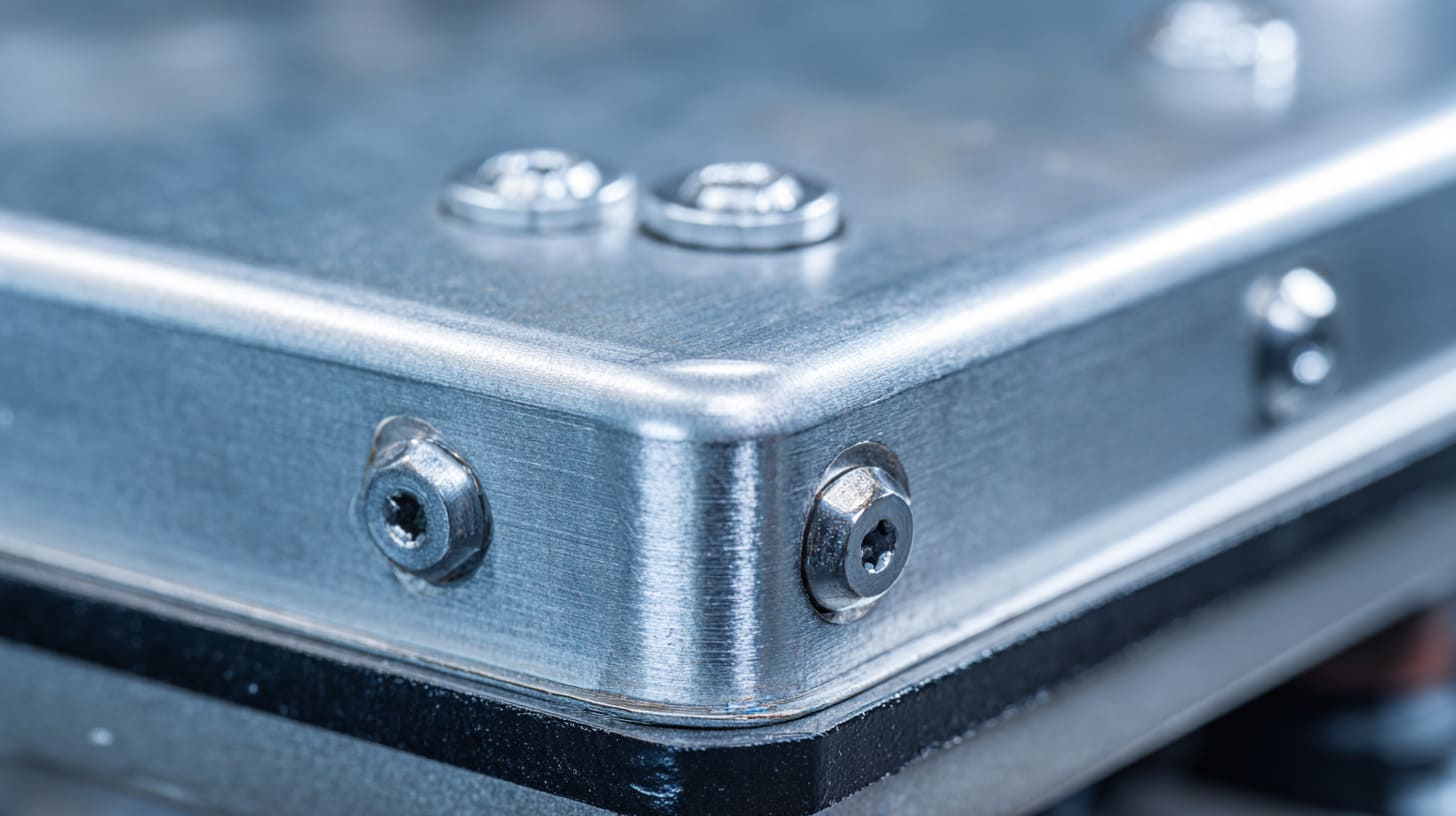
A lot of enclosure discussions go wrong because people think shielding is only about material choice. They say, “It is aluminum, so it should shield well.” That sounds reasonable at first. But shielding is not only about having metal. Shielding is also about how well that metal stays electrically connected where it needs to.
I have seen aluminum enclosures fail not because aluminum was the wrong material, but because the conductive path across the enclosure was weak, interrupted, or unstable.
One thing I judge very quickly is whether the design relies on theory or on real contact, because EMI problems usually punish theory first.
Role of Surface Conductivity in Shielding
At a basic level, an enclosure shields by helping redirect or contain electromagnetic energy. For that to happen well, the conductive shell has to behave like a continuous path, not like a collection of separate metal pieces that merely look connected.
This is especially important at the outer surface. At higher frequencies, current tends to stay near the surface. That means surface condition becomes very important. If the surface path is interrupted by insulating layers, gaps, coatings, or unstable contact points, shielding performance can drop.
I like to think of it this way: a metal enclosure is not just a box. It is an electrical path wrapped around a product.
If that path is broken in ten tiny places, the enclosure may still look beautiful. But electrically, it starts acting less like a shield and more like a leaky shell.
Importance of Contact Interfaces
The biggest problems usually hide at interfaces.
Seams matter. Joints matter. Screw points matter. Lid-to-base contact matters. Areas around cutouts matter too. A lot of leakage happens not through the middle of a metal wall, but through the places where one metal part meets another.
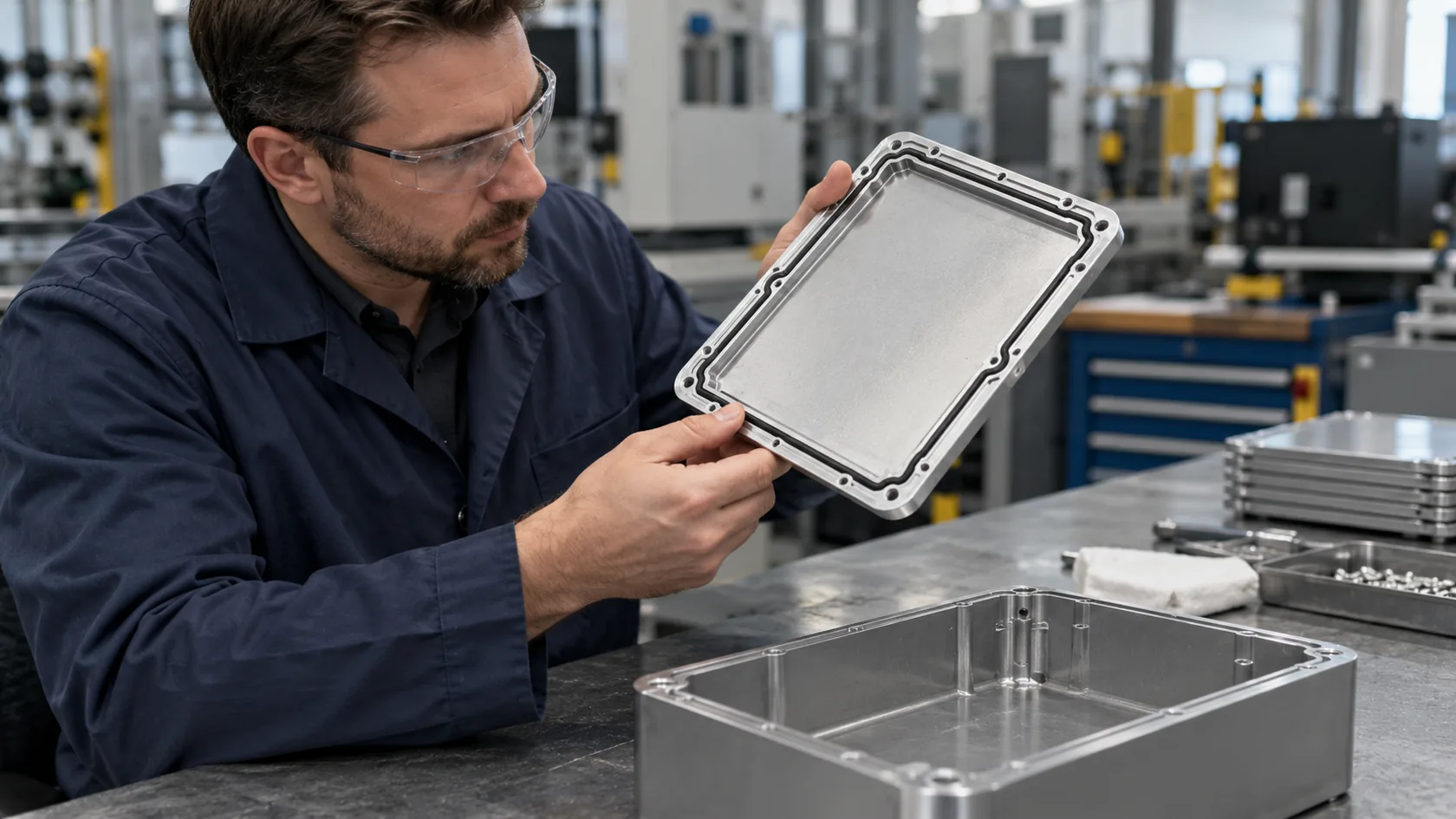
This is where many projects become misleading. The contact may look solid by eye, but electrical contact happens at a much smaller level. Surface roughness, coating thickness, pressure, torque, and finish all affect it.
Here is a useful comparison:
| What People See | What EMI Actually Cares About |
|---|---|
| The lid sits flush | Whether current can cross the seam |
| The screws are tight | Whether the contact resistance is low enough |
| Both parts are aluminum | Whether the oxide layer blocks continuity |
| Assembly feels strong | Whether shielding is stable across the whole enclosure |
That is why I do not trust visual neatness as proof of EMI safety. A pretty seam is not the same thing as a conductive seam.
High-Frequency Behavior
High-frequency behavior makes the problem worse.
At low frequencies, some weaknesses may stay hidden longer. At higher frequencies, small discontinuities start to matter much more. A tiny interruption in conductive continuity can create leakage. A seam that seems harmless on paper can become the exact place where the enclosure starts losing control.
This is one reason EMI-sensitive products need a different level of discipline. Once frequency rises, good-enough thinking becomes dangerous. A finish that works fine for a decorative enclosure may become a real liability for an RF-sensitive or certification-driven design.
I have noticed that long seams, repeated fastener points, and multiple mating surfaces often turn into bigger risks than buyers expect, especially when every exposed metal surface has been anodized without any conductive plan.
That leads straight to the real project question: when does full anodizing stop being a nice finish choice and start becoming a problem?
When Full Anodizing Becomes a Problem
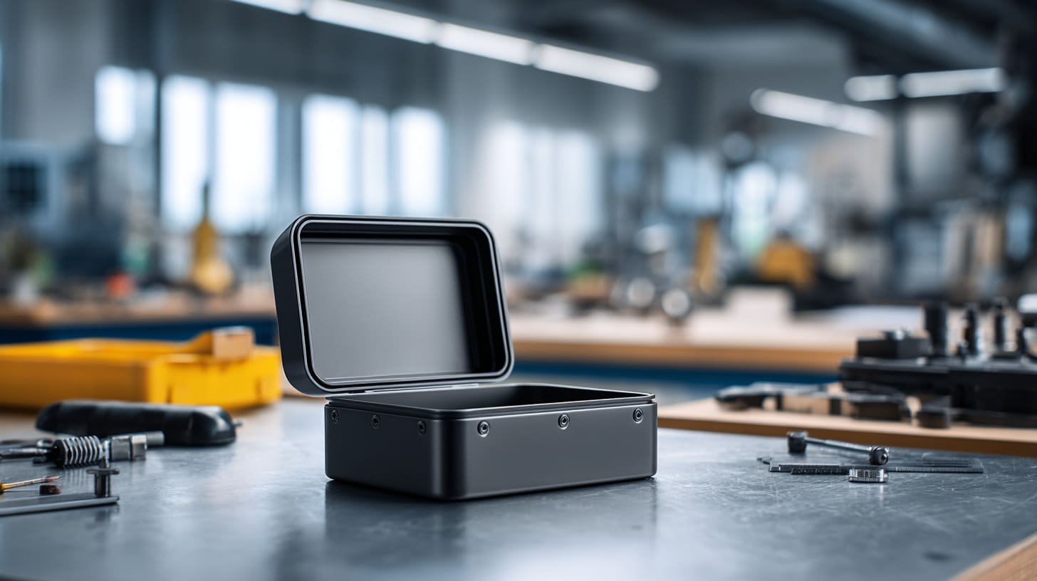
This is the part that matters most in real work. I do not reject full anodizing because of theory alone. I reject it when the enclosure design depends on conductive contact in places where anodizing gets in the way. That is the practical line for me.
Sometimes the risk is obvious. Sometimes it hides inside a design that looks completely normal. That is what makes this issue tricky.
My own warning light comes on when I see several contact-dependent features stacked together, because one weak seam is manageable, but five weak contact zones can turn into a test disaster.
Case 1: Multi-Part Enclosures with Seams
A multi-part enclosure is one of the clearest cases where full anodizing can become a problem.
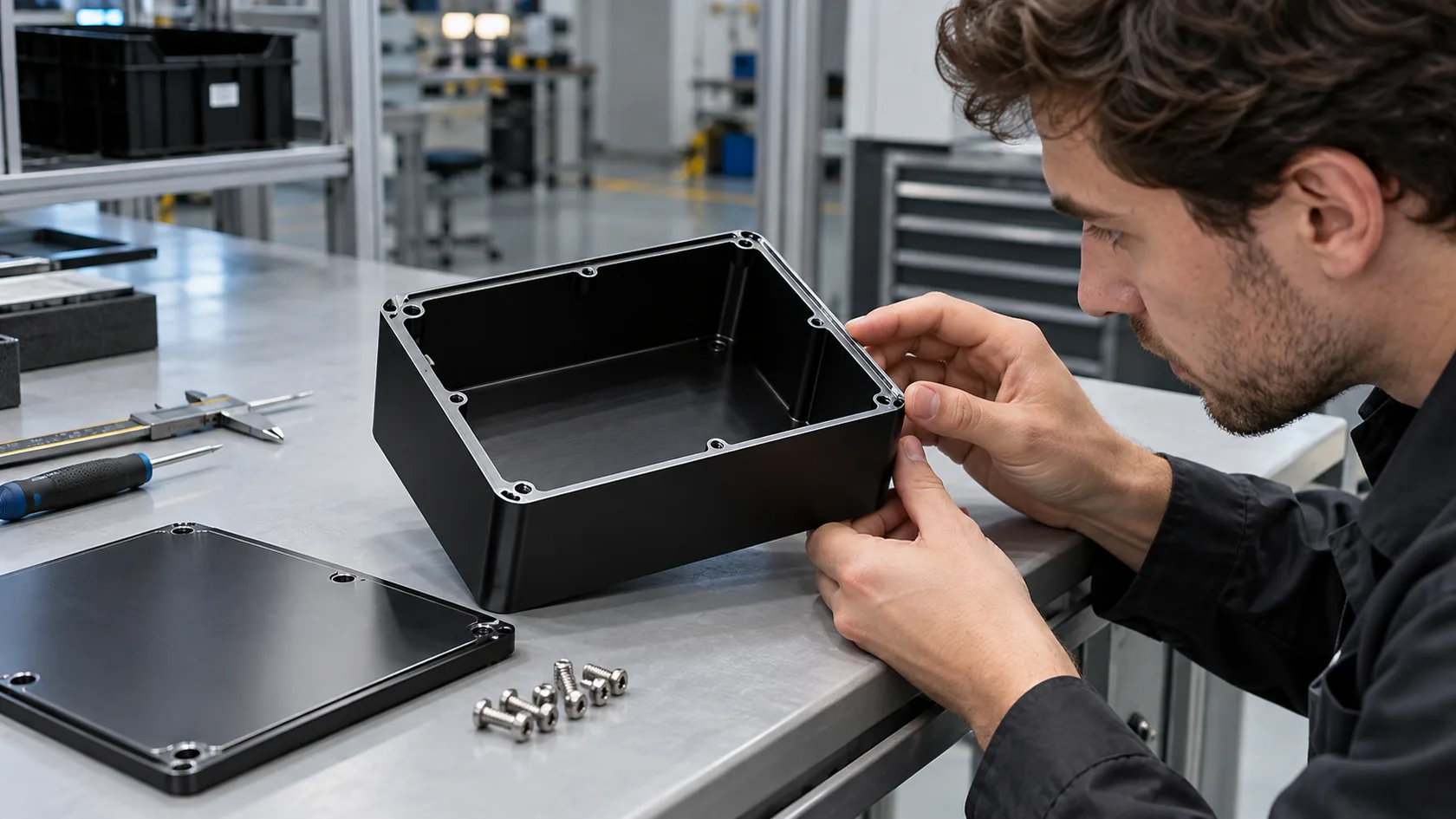
When a lid meets a base, or when two shells join together, the shielding path often depends on contact across that seam. If both surfaces are fully anodized, the oxide layer interrupts direct metal-to-metal electrical connection. The parts may still touch physically, but the conductive path may be poor or unstable.
This matters even more when the seam runs a long distance.
| Enclosure Type | Risk Level with Full Anodizing | Why |
|---|---|---|
| One-piece body with minimal seams | Lower | Less dependence on surface-to-surface contact |
| Two-part lid and base | High | Seam continuity becomes critical |
| Multi-panel assembly | Very high | Many contact interfaces increase leakage risk |
I have seen buyers assume that more screws automatically solve this. Sometimes they help. Sometimes they only compress two insulated surfaces more tightly.
Case 2: Screw-Fastened Structures
Screw-fastened structures create another common trap.
People often assume the screw itself will establish grounding and continuity. That can happen, but not reliably if anodizing remains under the screw head, around the mating area, or along the main seam path. A screw can create a localized break-through point, but that does not mean it creates a stable low-resistance path across the whole interface.
Pressure matters. Washer type matters. Contact area matters. Surface preparation matters too.
Here is how I compare common screw-area assumptions:
| Assumption | Reality |
|---|---|
| “The screw is metal, so grounding is fine” | Local contact may exist, but full seam continuity may still be poor |
| “More torque will solve it” | Too much torque can deform parts without guaranteeing stable conductivity |
| “The screws passed sample assembly” | Production variation can still create inconsistent EMI results |
I get especially cautious when the drawing has standard screw fastening but says nothing about teeth washers, masking zones, or designated grounding points.
Case 3: High-Frequency or Strict EMC Requirements
When the product works at higher frequencies, or when certification margins are tight, full anodizing becomes much harder to justify.
At that point, small losses in conductive continuity can turn into real compliance risk. A weak seam may not cause total failure every time, but it can shrink your safety margin. And small safety margins are expensive. They lead to repeated tests, redesign delays, and awkward conversations between engineering, sourcing, and management.
This is where many teams regret treating finish choice as a cosmetic issue.
If the product needs CE, FCC, or another strict EMC target, I do not like leaving conductive contact to chance. That is simply too expensive a gamble.
Case 4: Large Panel or Long Seam Designs
Large panels and long seams magnify the problem.
A small contact issue over a short distance may be tolerable. The same issue repeated over a long enclosure edge becomes much more serious. Long seams create more opportunities for poor contact, tiny gaps, and uneven pressure distribution. That means leakage risk builds up across the enclosure.
I have seen long rack-style housings and broad cover plates create trouble even when the finish and machining both looked professional. The longer the seam, the less I trust a passive assumption like “assembly pressure will handle it.”
That also explains why some failures feel strange at first. The enclosure looks solid. The hardware count seems fine. Yet the EMI result says otherwise. When that starts happening, the symptoms tend to leave clues.
Typical Failure Symptoms You Should Recognize
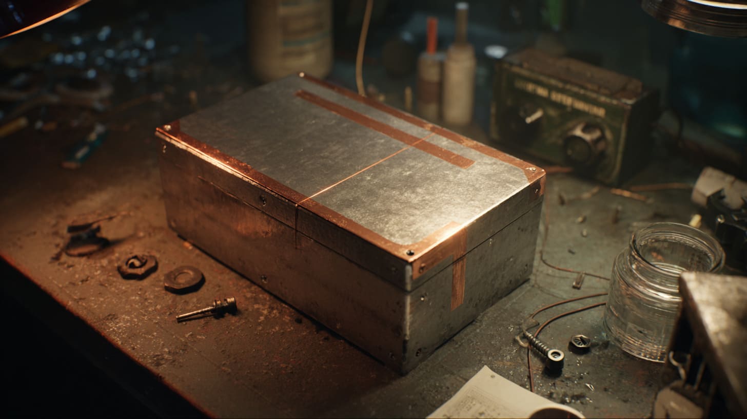
EMI finish problems rarely introduce themselves politely. They usually show up as confusing symptoms. The enclosure looks fine. The assembly team says it feels normal. The first instinct is to blame the PCB, the cable, or the grounding layout. Sometimes that instinct is right. But not always.
I have learned to pay attention to patterns, because enclosure-related EMI trouble often leaves fingerprints before it leaves a final conclusion.
What makes me pause is not one strange test number, but a pattern where the enclosure behaves worse than it looks.
Unexpected EMC Test Failures
One of the clearest warning signs is a product that passes visual inspection but struggles in EMC testing.
That mismatch matters. If the machining is good, the assembly is neat, and the material is conductive in theory, then I start asking hard questions about seams, contact resistance, and surface finish. Full anodizing often enters the conversation at that point.
A common pattern looks like this:
- The enclosure appears robust
- The product fails at certain frequencies
- Basic electrical functions still work normally
- Quick conductive fixes improve the result
That last point is important. If a crude conductive patch improves shielding, the original contact path was probably weaker than people thought.
Sensitivity to Assembly Variations
Another clue is unusual sensitivity to assembly changes.
A product may perform one way when one technician assembles it and another way when someone else does the same job with slightly different torque or sequence. That is not a comforting sign. Stable EMI performance should not depend too much on small human differences.
Here is a useful symptom table:
| Symptom | What It May Suggest |
|---|---|
| Different test results across builds | Unstable contact path |
| Better result with higher screw torque | Weak seam conductivity |
| Better result after reassembly | Contact inconsistency |
| Strong dependence on washer type | Poor base conductive interface |
When I see that kind of variability, I stop blaming luck. I start checking whether the finish is preventing repeatable conductivity.
Temporary Fixes That “Work Too Well”
This is one of my favorite warning signs because it is so revealing.
If copper tape, conductive gasket material, scraped contact spots, or temporary bare-metal exposure suddenly improve the result, that is not a random victory. It usually means the enclosure was missing a reliable conductive path from the start.
I do not love these emergency fixes as permanent solutions, but I respect what they reveal. They tell me where the real weakness is.
A simple way to read the situation is this:
| Temporary Fix | Likely Message |
|---|---|
| Copper tape on seam helps | Seam conductivity was weak |
| Conductive gasket helps | Contact pressure or coating was limiting current flow |
| Scraping anodized spots improves result | Oxide layer was blocking the path |
| Extra bonding wire helps | Natural enclosure continuity was not enough |
Once those clues show up, the next step is not panic. The next step is judgment. Because full anodizing is not always wrong. There are cases where it is perfectly acceptable.
Situations Where Full Anodizing Is Still Acceptable
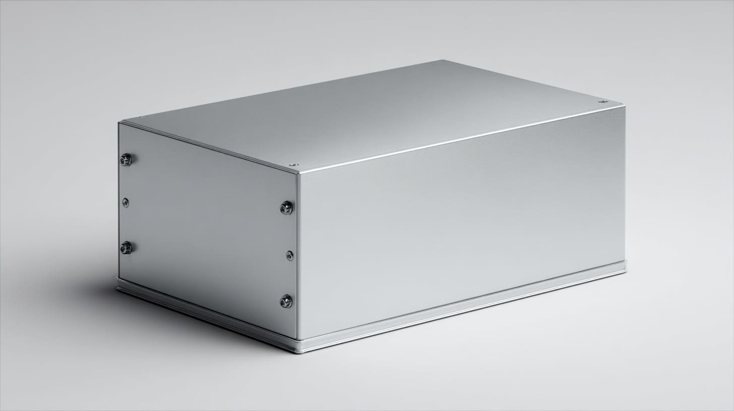
I do not want to make this sound absolute. Full anodizing is not a mistake by default. It becomes a mistake only when the EMI role of the enclosure conflicts with the electrical effect of the finish. In many products, that conflict is weak or manageable.
The real issue is context.
I often approve full anodizing without much hesitation when the shielding job is modest and the enclosure is not being asked to carry a demanding conductive role.
Non-EMI-Critical Applications
Some enclosures simply do not face strict EMI pressure.
Decorative housings, basic industrial covers, low-frequency devices, and products with little sensitivity to external noise can often use full anodizing without serious trouble. In those cases, corrosion resistance and appearance may matter much more than conductive seam continuity.
That does not mean EMI can be ignored. It just means the finish choice is less likely to become the dominant risk.
Fully Sealed or Welded Structures
A fully sealed or welded structure is a different story from a screw-fastened multi-part housing.
If the conductive body is already continuous through welding or another strong structural method, the outside anodized layer may not matter as much. The enclosure is not relying on repeated surface contact across multiple seams to build its shielding path. That changes the risk level a lot.
I am much less worried when the enclosure has very few electrical contact dependencies at assembly interfaces.
Internal Shielding Solutions Used
Some products rely on internal shielding measures instead of depending mainly on the outer enclosure finish.
These may include conductive coatings inside the shell, shielding cans over sensitive circuits, EMI gaskets in controlled locations, or dedicated grounding strategies. In that case, the anodized exterior becomes less important to the main shielding function.
Still, I do not assume internal shielding makes finish choice irrelevant. I check whether the internal solution is truly robust or just a weak backup.
Here is how I roughly judge it:
| Situation | Is Full Anodizing Usually Acceptable? | My View |
|---|---|---|
| Decorative or non-EMI-critical enclosure | Yes | Usually low concern |
| Welded conductive body | Often yes | Risk depends on openings and interfaces |
| Strong internal shielding design | Often yes | Must verify real effectiveness |
| Multi-part EMI-sensitive enclosure | Often no | Needs extra caution |
Once I reach the point where full anodizing looks risky, the useful question is no longer “Should I give up protection and appearance?” The better question is, “What finish strategy gives me both control and performance?”
Better Alternatives to Full Anodizing for EMI Designs
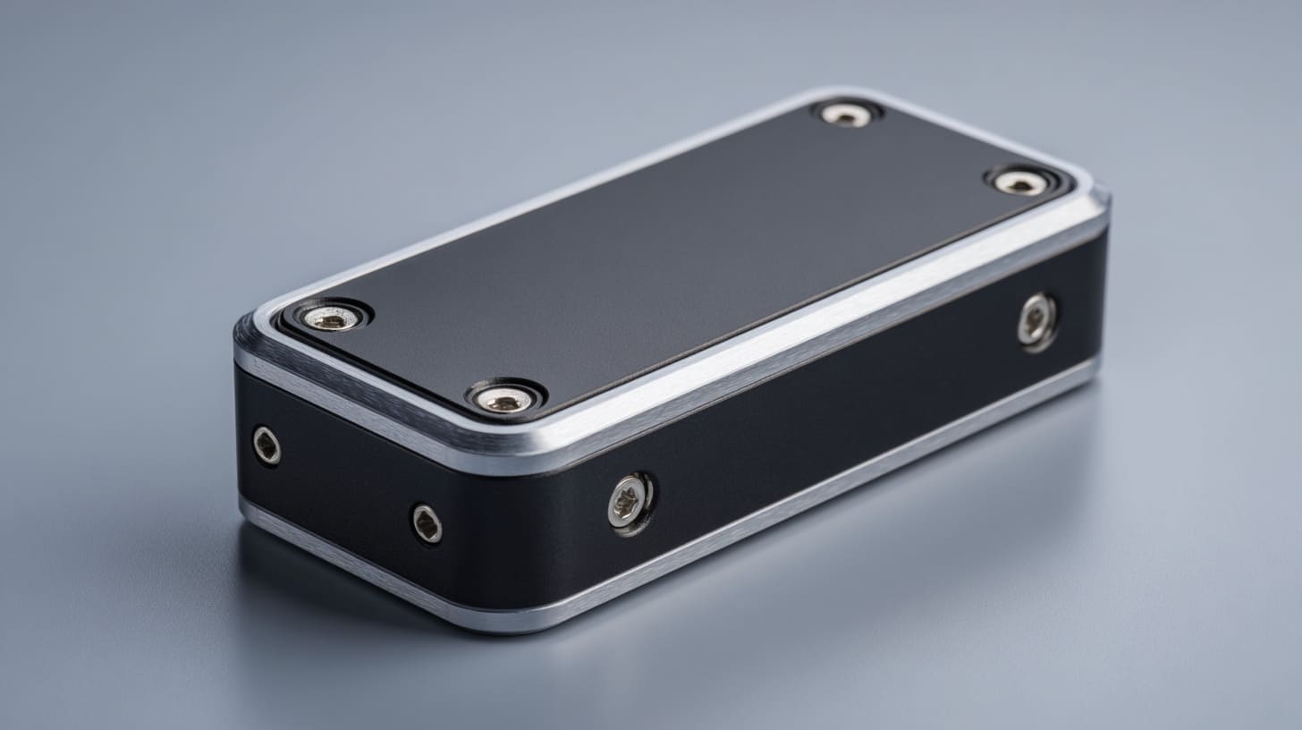
This is where good enclosure work gets more interesting. I do not like false choices. I do not want to pick between corrosion protection and EMI performance if I can avoid it. In many projects, I do not have to. The smarter answer is often a more controlled surface strategy.
I tend to trust solutions that make the conductive path intentional, because accidental conductivity is rarely as reliable as planned conductivity.
Selective (Masked) Anodizing
Selective anodizing is one of the most practical answers.
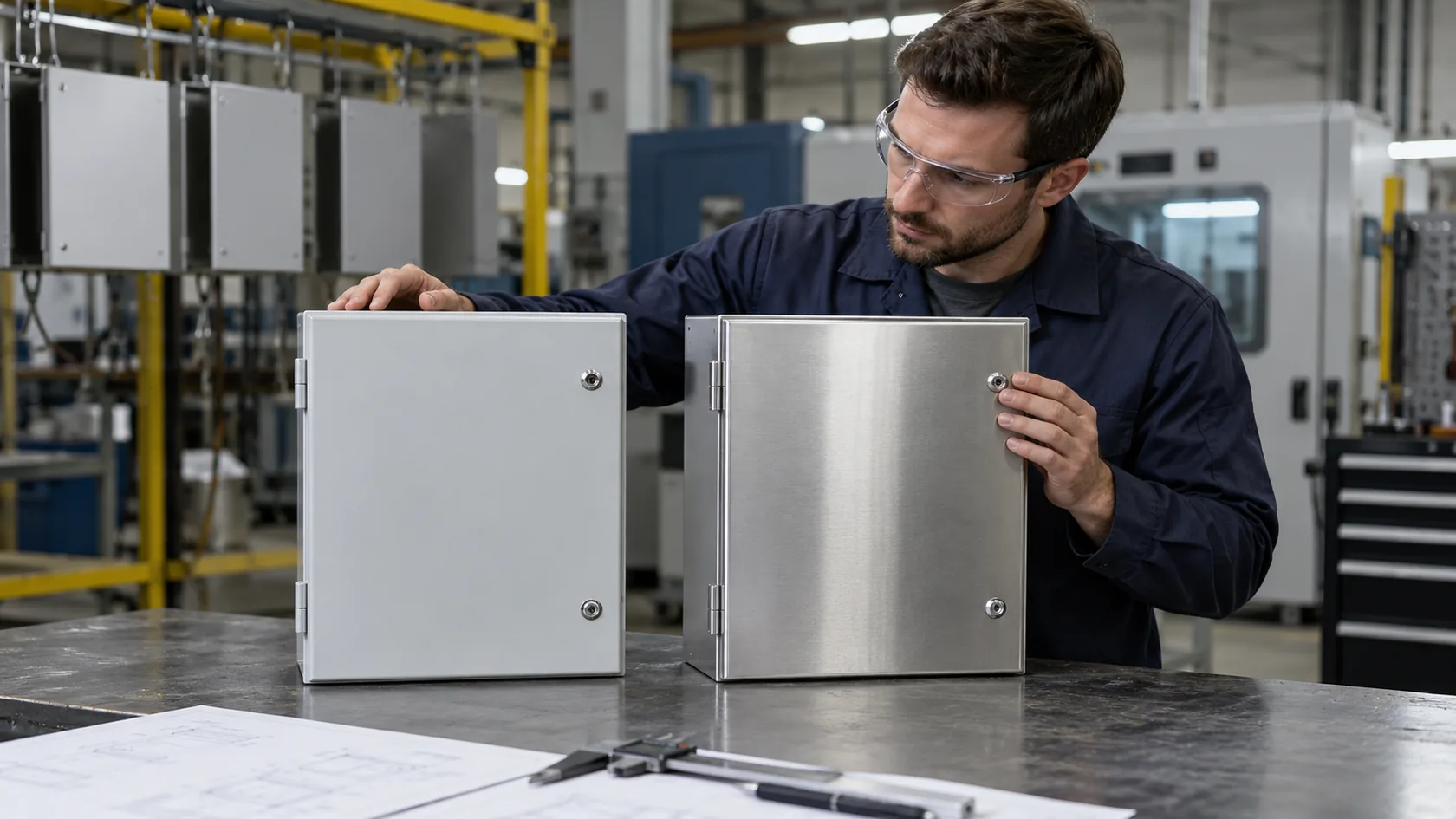
In this approach, the enclosure still gets anodized in the areas where appearance and protection matter, but key contact zones are masked or kept bare. That way, I preserve conductivity where the EMI path depends on it.
These areas often include:
- Seam contact lands
- Grounding pads
- Screw seating zones
- Gasket interface areas
- Bonding points
This method gives a better balance between finish quality and shielding performance. It is not always the cheapest process choice, but it often saves far more money than a failed EMC redesign.
Conductive Conversion Coatings
Conductive conversion coatings are another strong option.
These coatings offer corrosion protection while keeping the surface conductive enough for electrical continuity. They do not look the same as anodizing, and buyers sometimes prefer the appearance of anodized parts. Still, when EMI matters more than visual perfection, conductive coatings often make more technical sense.
Here is a basic comparison:
| Finish Option | Corrosion Protection | Appearance | Conductivity | EMI Suitability |
|---|---|---|---|---|
| Full anodizing | High | High | Low | Weak unless compensated |
| Selective anodizing | High | High | Controlled | Stronger |
| Conductive conversion coating | Medium to high | Medium | High | Strong |
| Raw aluminum | Low | Low | High | Strong, but poor durability |
Mechanical Design Optimization
Finish choice is not the only lever. Mechanical design matters too.
A better seam geometry can improve shielding. Teeth washers can help break through surface films in specific zones. Conductive gaskets can create more reliable contact. Better fastener spacing can reduce leakage opportunities. Higher and more even contact pressure can also help.
Still, I try not to use mechanical tricks as an excuse for a bad finish decision. They should support the conductive plan, not replace it.
Hybrid Surface Strategies
Sometimes the best answer is a hybrid strategy.
I may keep the exterior anodized for customer-facing appearance and corrosion resistance, while preserving internal or interface zones for conductivity. That gives the product a polished look without sacrificing the electrical path where it actually matters.
That kind of solution usually feels more mature to me than full anodizing everywhere or raw aluminum everywhere. It shows the design was thought through.
And once alternative options are on the table, the next challenge becomes judgment: how do I decide before approval, not after failure?
Design Decisions: How to Judge Before Approval

This is where I think the real value sits. A lot of EMI enclosure mistakes happen not because the team lacked intelligence, but because the finish decision got approved too early and questioned too late. Once parts are finished, assembled, branded, and scheduled for testing, even a small surface issue becomes expensive.
I make better decisions when I force the finish discussion to happen before people become emotionally attached to the cleanest-looking option.
Ask About EMI Requirements Early
I always want the EMI target defined early.
That means I need to know the frequency range, the sensitivity of the product, the certification target, and how much shielding margin the design is expected to carry. If those answers are vague, then approving full anodizing becomes riskier because the finish is being chosen without a clear performance boundary.
A simple early checklist helps:
| Question | Why I Ask It |
|---|---|
| What standard must the product meet? | Finish risk depends on compliance pressure |
| What frequency range matters most? | Higher frequencies punish weak interfaces more |
| Is the enclosure part of the shielding strategy? | If yes, finish choice becomes critical |
| Is there margin for redesign? | If no, I avoid risky assumptions |
Evaluate Contact Path Design
I look carefully at the contact path.
Where does current need to travel? Which seams matter? Which screws are functional for grounding and which are only structural? Are there gasket lands? Are there bare contact zones? If the answer to these questions is unclear, I do not trust the finish decision.
This is where rough drawings often hide expensive problems. A product can be well-designed electrically and still suffer because the contact plan at the enclosure level was never really defined.
Check Finish Specification Details
I also check the finish note itself, because vague finish language causes real trouble.
“Black anodize” is not enough detail on an EMI-sensitive enclosure. I want to know whether masking is required, where it is required, what thickness is expected, and whether the supplier understands which zones are functional contact areas.
This is where many buyer-supplier problems begin. One side thinks the finish is cosmetic. The other side thinks it is technical. Then nobody clearly defines the interface zones.
Prototype and Test Strategy
I believe strongly in early prototype testing.
A pre-test costs far less than a delayed launch. If the finish is part of the risk, I would rather test an early sample with realistic surface treatment than wait until the final build. That is especially true when the enclosure has multiple seams, high-frequency exposure, or strict EMC requirements.
This is the question I ask myself before approval: am I choosing a finish because I know it will work, or because I hope it will?
When that question becomes uncomfortable, it usually means I need to slow down and look for mistakes that people commonly make at this stage.
Common Mistakes Buyers and Engineers Make
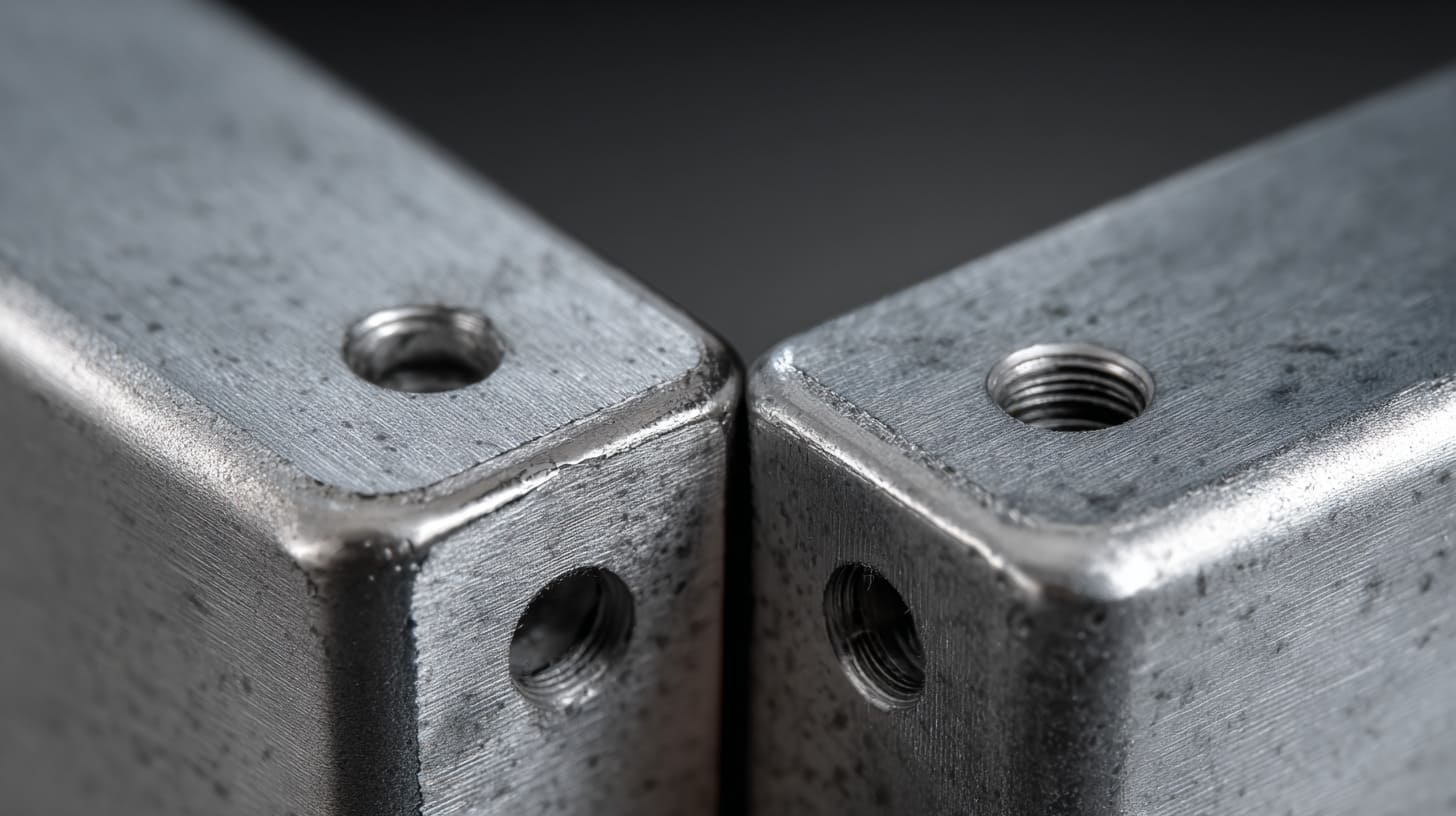
I do not say this to criticize buyers or engineers. I say it because I have seen smart people make the same mistakes again and again. I have made some of them myself. EMI problems around anodizing are usually not caused by laziness. They are caused by assumptions that feel reasonable until real hardware proves otherwise.
The mistake I see most often is simple: people give visual quality more trust than electrical reality.
Treating Anodizing as Purely Cosmetic
This is probably the biggest mistake.
People think of anodizing as color, hardness, and brand feel. They forget it is also a surface condition with electrical consequences. Once that happens, the finish note gets treated like a styling note instead of a functional decision.
I understand why this happens. Appearance is easier to discuss. EMI behavior is less visible. But invisible problems still cost money.
Assuming “Metal Touching Metal” Is Enough
This assumption sounds harmless, but it has caused plenty of trouble.
Two metal parts touching each other does not guarantee good electrical continuity if oxide layers, poor pressure distribution, or finish buildup are involved. Mechanical contact and electrical contact are related, but they are not the same thing.
I get nervous when someone points at a CAD assembly and says, “It’s all aluminum, so it should be fine.” That sentence has misled too many projects.
Ignoring Supplier Process Details
Another common problem comes from incomplete communication with the supplier.
The buyer may understand that conductivity matters. The factory may understand anodizing. But if nobody clearly marks masking zones, grounding areas, finish limits, and inspection expectations, the finished part may still come back wrong.
This matters even more in custom projects where drawings, comments, and samples move between teams in different countries and time zones.
A small process detail can change the result a lot:
| Missed Detail | What Can Go Wrong |
|---|---|
| No masking note | Contact areas get fully anodized |
| No finish thickness control | Contact resistance becomes inconsistent |
| No defined ground point | Assembly team guesses the conductive path |
| No EMI-focused inspection | Visual acceptance hides electrical weakness |
Delaying EMI Consideration Until Testing Stage
This is the most expensive mistake of all.
When EMI is treated as a final test event instead of a design input, surface finish errors become much harder to fix. At that point, the enclosure may already be machined, finished, assembled, packed, and promised to customers.
I have seen teams lose time not because the fix was technically impossible, but because it arrived too late.
That is why I push this decision earlier than some people expect. It is easier to argue over masking lines on a drawing than to explain a failed certification report after production has already moved.
And that brings me to the real conclusion, the one I have reached not from theory alone, but from how these projects behave in real life.
Conclusion
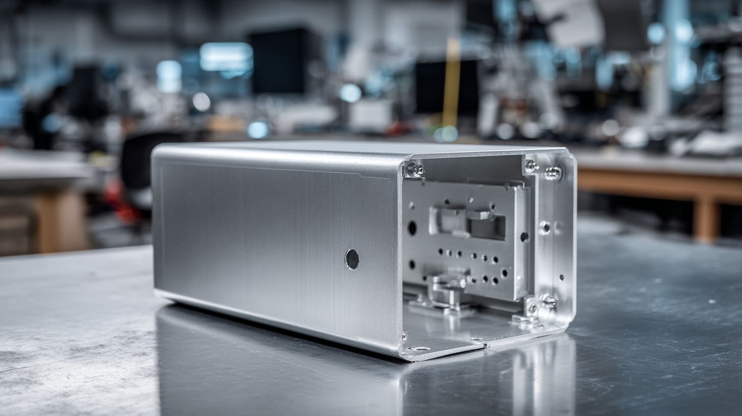
I do not reject full anodizing because I dislike anodizing. I reject it in certain EMI-sensitive enclosure projects because I have seen what happens when a finish that looks smart on paper quietly damages the conductive path the enclosure depends on. That is the heart of my view.
For me, this decision is about judgment, not habit.
If an enclosure mainly needs appearance, wear resistance, and corrosion protection, full anodizing can be a very reasonable choice. I have no problem saying yes in that kind of case. But when the enclosure also needs to act like a reliable EMI shield, I stop looking at anodizing as a harmless default. I start asking harder questions about seams, contact zones, screw interfaces, frequency range, and compliance margin.
The reason I think this way is simple. I have learned that EMI failures are rarely dramatic at the beginning. They start as tiny oversights. A finish note gets written too broadly. A seam contact area gets forgotten. A sample looks beautiful. Then the test result exposes the weak point. By then, the “small” finish choice is no longer small.
So when do I think you should not approve full anodizing on an EMI-sensitive enclosure?
I would say no when the design depends on conductive continuity across seams, fasteners, and mating surfaces, and no one has clearly protected those paths. I would also say no when the EMC target is strict, the seam structure is long or complex, and the finish decision is being made on appearance alone. In those cases, full anodizing is not just a finish choice. It becomes a hidden electrical risk.
What I trust more is controlled intent. Mask the contact zones. Use conductive coatings where needed. Define the grounding path clearly. Test early. Give the surface finish the same seriousness you give the PCB and the grounding layout. That is how I avoid expensive surprises.
If you are working on an EMI-sensitive enclosure project and you are not sure whether full anodizing is helping or hurting, send the drawing or project details to me. I can help you review the seam design, contact areas, and finish approach before you commit to production. That kind of check is much cheaper than learning the answer in the test chamber.