Skip to content
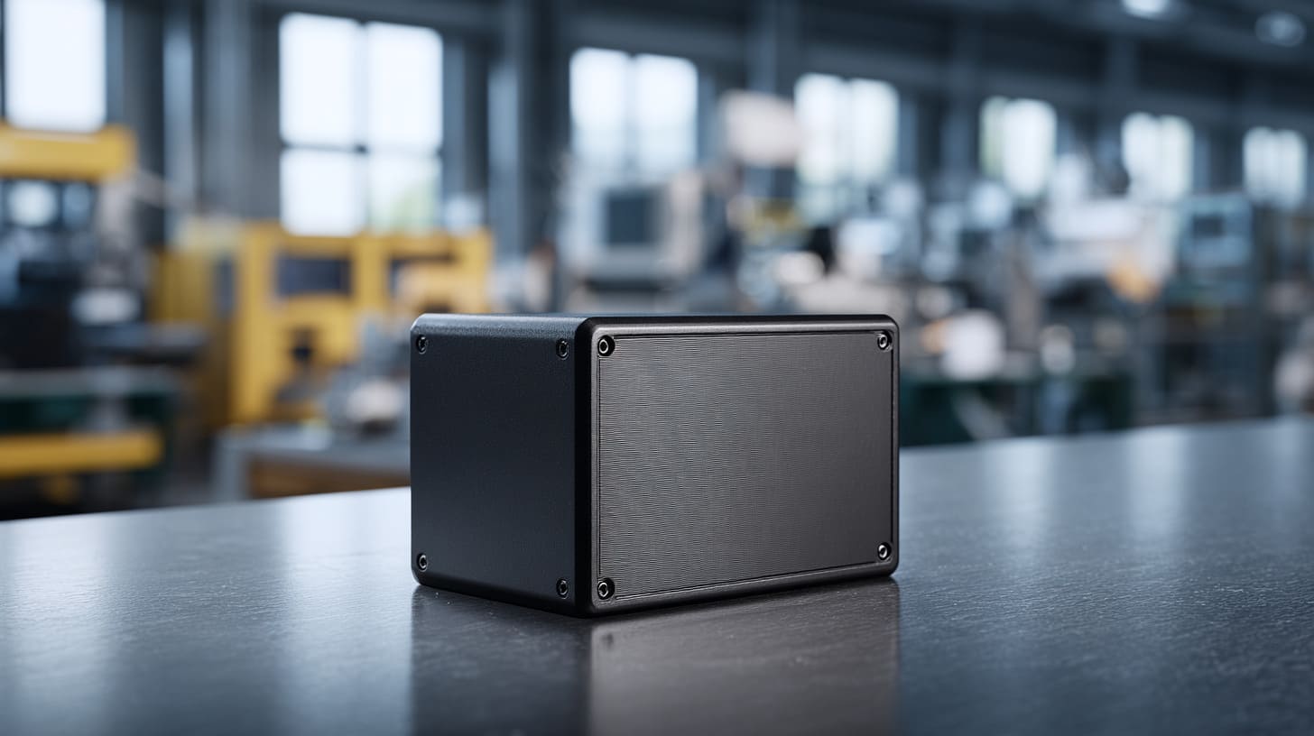
A clean anodized aluminum enclosure can make people relax too early.
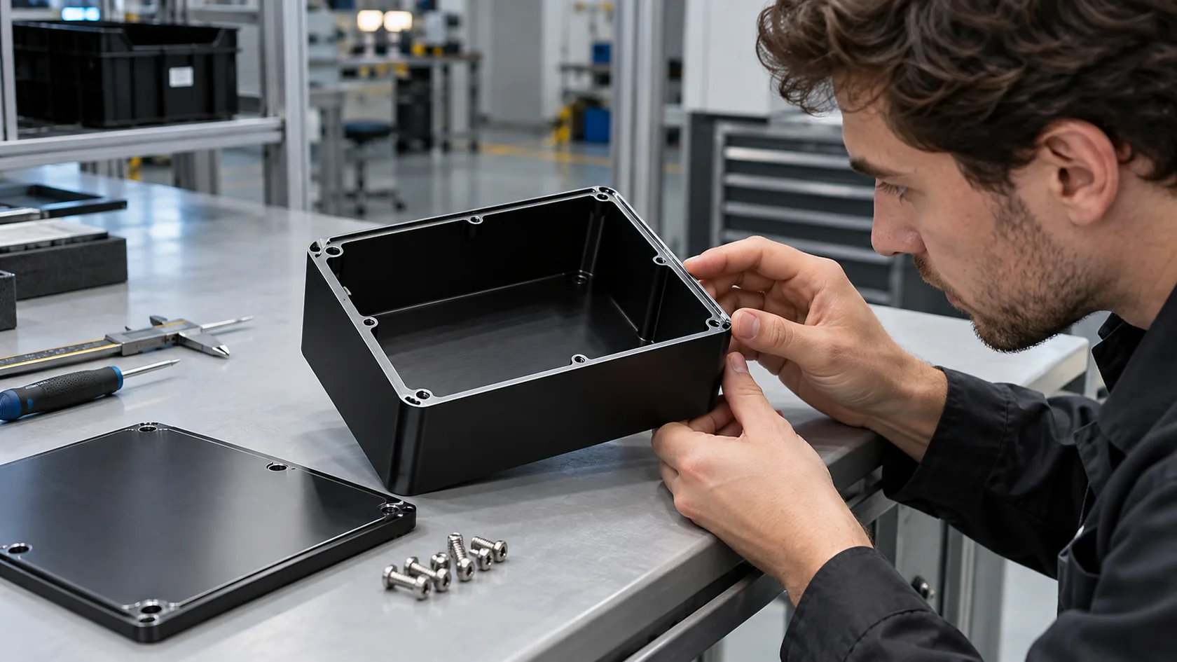
I have seen that reaction many times. The surface looks even. The color looks serious. The edges feel neat. The case gives off that quiet message buyers like to hear: this product is under control. That feeling is real. I understand it. I work with custom enclosures all the time, and I know how much a good surface finish can change the whole impression of a product.
But this is also where people get fooled.
A case can look premium and still create trouble. A product can pass the eye test and still fail the EMC test. That gap matters more than many teams expect. I have seen engineers spend days looking at the PCB, the cable, and the grounding wire, only to find out the real issue was hiding in the enclosure seam the whole time.
The problem is simple, but it hides well. Full anodizing on mating surfaces can break electrical continuity. The enclosure still looks like metal. It still feels like metal. But electrically, some key contact areas stop behaving the way the team assumes.
That is why I do not judge enclosure safety by appearance anymore. A rough raw contact zone often gives me more confidence than a perfectly colored seam with no real conductive path.
For buyers, this matters because the risk does not show up nicely in drawings. For product engineers, this matters because one surface decision can affect shielding, bonding, testing time, and project cost. For suppliers like me, this matters because a “beautiful sample” can become a painful production lesson later.
I think this topic deserves more honesty. Not the glossy version. The real version.
The funny thing is that many EMC problems do not start with loud mistakes. They start with smart-looking decisions. That is why I want to slow down here and begin with the surface itself.
What Is Anodizing and What Does It Really Do?

Anodizing sounds simple when people talk about it fast. It is often treated like a nice finishing step. Add color. Add corrosion resistance. Improve wear. Make the enclosure look better. That is all true. Still, it is not the full story.
I prefer to describe anodizing in a more honest way. It is not just decoration. It changes the surface of aluminum in a very real way.
What happens during anodizing
Anodizing is an electrochemical process. The aluminum part goes through a treatment that grows an oxide layer on the surface. This layer is not paint sitting on top like dust on a table. It becomes part of the surface itself.
That is why anodizing feels durable. It is also why it can create confusion. People see metal under the finish, so they assume the whole thing still behaves like exposed aluminum. It does not.
In normal enclosure work, anodized thickness can vary by application. Some projects need a lighter finish for appearance. Some need a harder finish for wear. Some need black, silver, blue, or custom colors for branding. The exact thickness may change, but one fact stays the same: the surface is no longer bare conductive aluminum.
Key properties of the anodized layer
The anodized layer does several useful jobs. I use it often for good reasons.
| Property | What it helps with | Why buyers like it |
|---|---|---|
| Corrosion resistance | Protects aluminum in daily use | Better durability in harsh environments |
| Wear resistance | Improves surface hardness | Better handling and longer service life |
| Appearance | Gives a clean and premium look | Better brand image |
| Color control | Supports black, silver, and other finishes | Easier product line matching |
| Electrical insulation | Reduces conductivity at the surface | Good in some uses, risky in others |
This is where things often go wrong: a feature that helps one goal can quietly hurt another one. A finish can improve corrosion resistance and still make EMC performance worse. That is not a contradiction. That is just engineering life.
Why anodizing is electrically non-conductive
The oxide layer formed by anodizing behaves like an insulator. That point sounds technical, but the practical meaning is easy to understand. If two anodized parts touch each other, they may look like two metal parts meeting. In reality, the contact is not clean metal-to-metal contact.
That changes everything for EMC.
At low expectations, the enclosure still seems fine. The lid fits. The screws tighten. The housing feels solid. But once high-frequency currents need a clean path across seams and joints, the truth comes out. The surface resistance becomes a problem.
I do not treat anodizing as a cosmetic decision anymore. I treat it as an electrical decision wearing a cosmetic disguise.
Here is a simple comparison I often use in my head:
| Surface condition | Mechanical appearance | Electrical behavior |
|---|---|---|
| Bare aluminum | Less refined | Good chance of conductive contact |
| Fully anodized aluminum | Very refined | Surface conductivity reduced |
| Masked contact area + anodized visible area | Balanced | Better for appearance and bonding |
That balance matters. Too many people only look at the second column.
A nice finish can make a project feel mature. Then the seam reminds everyone that physics does not care about style. So the next question becomes unavoidable: where exactly does this risk live on the enclosure?
What Are Mating Surfaces in Enclosures?
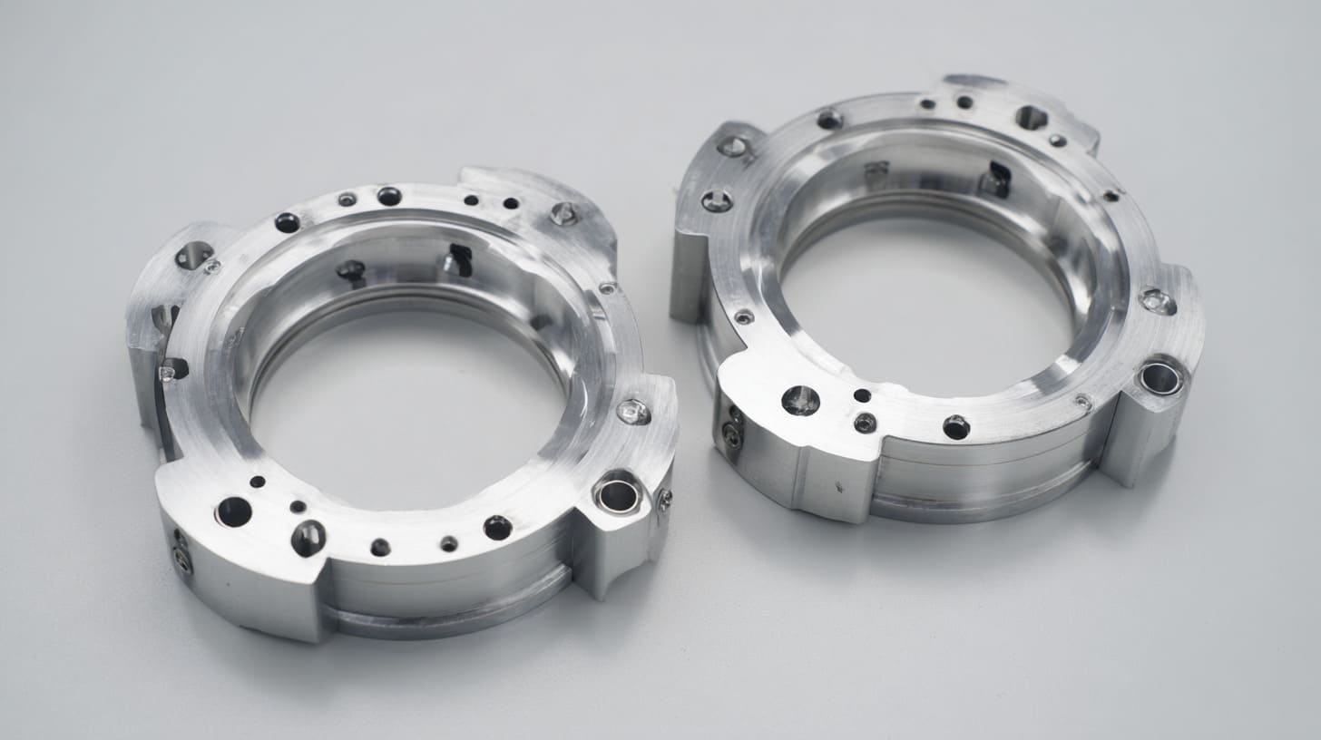
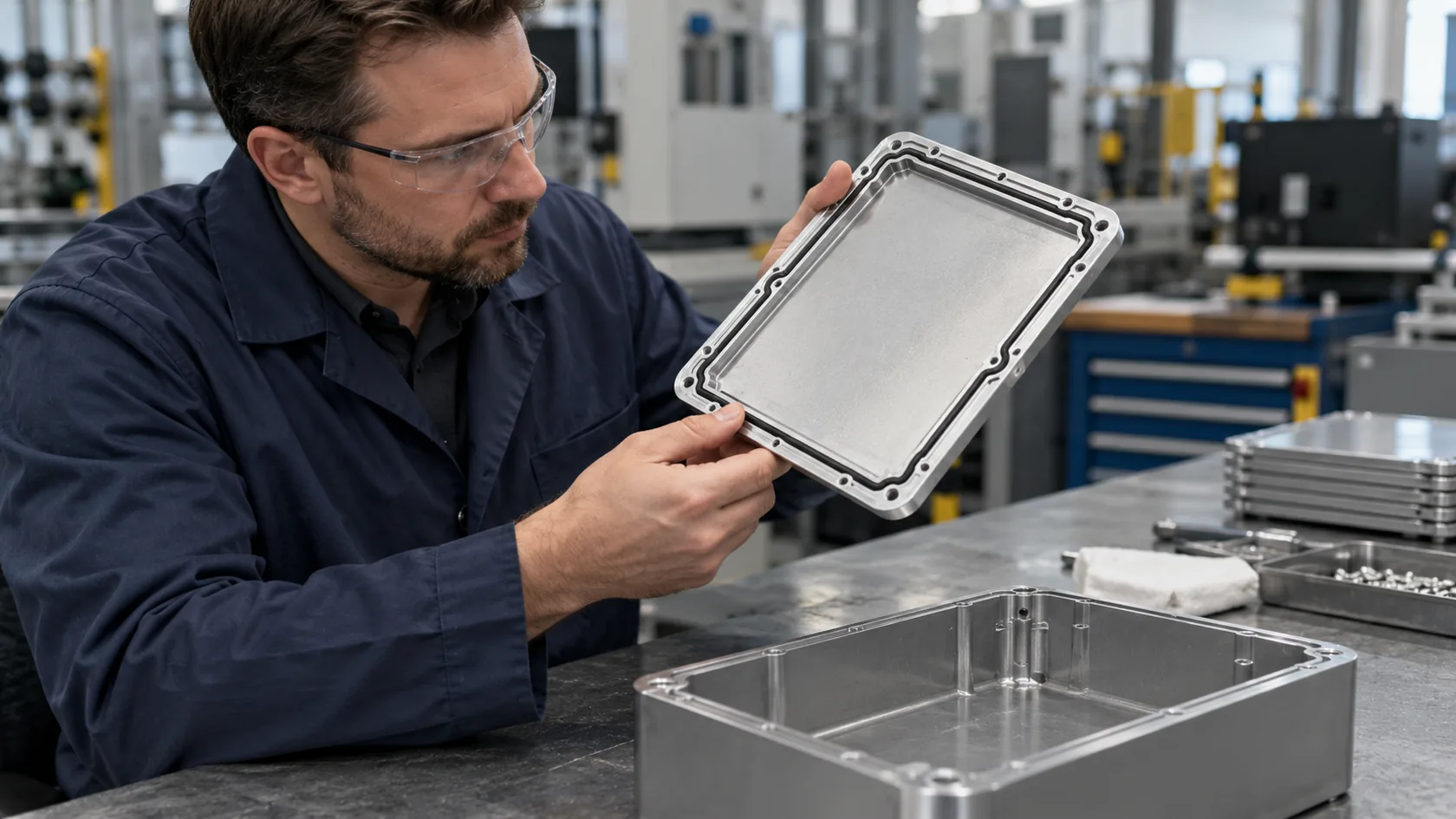
When I say mating surfaces, I do not mean something fancy. I mean the places where one enclosure part meets another. That is all. Still, those simple contact zones carry more responsibility than many drawings suggest.
I have seen teams spend a lot of time on wall thickness, bend radius, logo position, and finish color. Those things matter. But the quiet little contact areas between lid and base often decide whether the enclosure behaves like one electrical body or a group of pretty parts pressed together.
Definition of mating surfaces
Mating surfaces usually include areas like these:
- Lid-to-base contact edges
- Panel-to-frame contact points
- Cover seams
- Screw seating zones
- Internal partition contact faces
- Joint flanges and overlaps
These areas may look small on paper. But in real work, they act like checkpoints. They decide whether electrical continuity can pass through the structure or stop at the surface layer.
Their role in enclosure design
Most people first think of mating surfaces as mechanical features. That is fair. They help alignment. They help assembly. They may support sealing. They may control gap size and product feel.
Still, in metal enclosures, they also matter for shielding and bonding.
I usually explain it this way: if the outer shell is supposed to behave like a shield, then all those joined surfaces need to act like parts of one shield, not strangers sitting side by side.
| Mating surface job | Mechanical view | EMC view |
|---|---|---|
| Lid meets base | Fit and alignment | Conductive path across seam |
| Screw connection area | Clamping force | Local bonding point |
| Internal divider contact | Assembly support | Internal current return path |
| Overlap seam | Appearance and stiffness | EMI leakage control |
A lot of enclosure trouble starts when the team only respects the left side of that table.
Where designers usually overlook them
The danger is not always in obvious places. The obvious seam may get attention. The hidden one may not.
I have seen these areas get ignored:
- Contact surfaces under screw heads
- Anodized inside lips that never appear in beauty shots
- Partition walls that touch only after assembly
- Narrow flange edges where tolerance stack-up changes contact quality
- Corners where the mechanical fit looks tight, but electrical contact is weak
My own habit is to look for the surfaces nobody is proud to show in the brochure. That is usually where the truth sits.
A clean outside view can hide a weak electrical joint inside. And once I start thinking about seams that way, the next step is obvious: I need to look at how shielding actually works, not how people imagine it works.
How EMC Shielding Works in Metal Enclosures
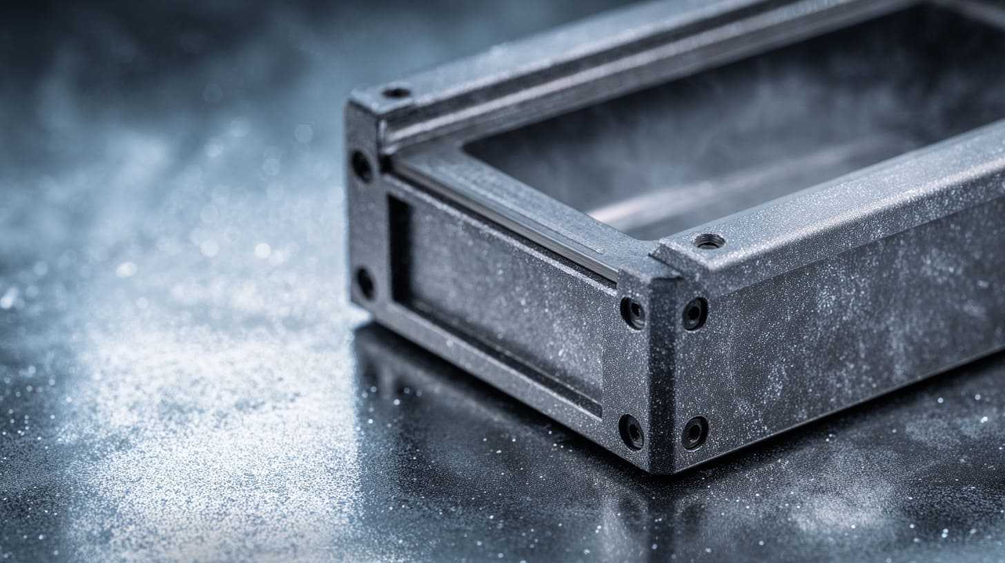
A metal enclosure does not block noise by magic. I say that because many people, even smart people, still talk about shielding as if metal alone solves everything. It does not. The enclosure has to behave like a continuous conductive body.
That word matters: continuous.
Basic principle of EMI shielding
A metal enclosure helps reduce electromagnetic interference by reflecting and guiding energy. People often describe this with the idea of a Faraday cage. That picture is useful, but only if we do not turn it into a lazy shortcut.
A cage only works well when it acts like a real enclosure, not a metal object full of weak joints and insulated contact points.
If the shell is continuous, unwanted energy has a harder time getting in or out. If the shell has bad seams, broken contact paths, or leakage points, the shielding effect drops.
Importance of continuous conductive paths
High-frequency current likes surface paths. It travels where the impedance is low. That means enclosure seams matter far more than many people expect. A weak seam can interrupt that path and force current to behave badly.
Here is a blunt truth I have learned: a case can be made of metal and still perform like a poor shield if its conductive path is broken at the joints.
This is one of those details I never ignore during enclosure review, because the project cost of “we assumed the seam was fine” is usually much higher than the cost of checking it early.
Role of seams and joints
Seams and joints are often the weakest part of a shielded enclosure. A tiny gap can act like a leakage point. At higher frequencies, even a small opening can cause trouble that feels strangely out of proportion to its size.
That surprises people. The gap looks tiny. The EMC failure looks big.
| Enclosure feature | Looks acceptable mechanically? | Can still hurt EMC? | Why |
|---|---|---|---|
| Tight lid seam | Yes | Yes | Tight fit does not guarantee conductivity |
| Painted contact zone | Yes | Yes | Coating interrupts metal contact |
| Fully anodized seam | Yes | Yes | Oxide layer adds resistance |
| Bare masked seam | Sometimes less pretty | Often better | Conductive contact is more likely |
I think the smartest way to read an enclosure is this: every seam is guilty until it proves itself electrically.
A lot of people understand shielding in broad terms. Fewer people follow that idea all the way to the finish treatment. That is where the trouble sharpens, because full anodizing does not just change color. It changes the path.
Why Full Anodizing Breaks EMC Performance
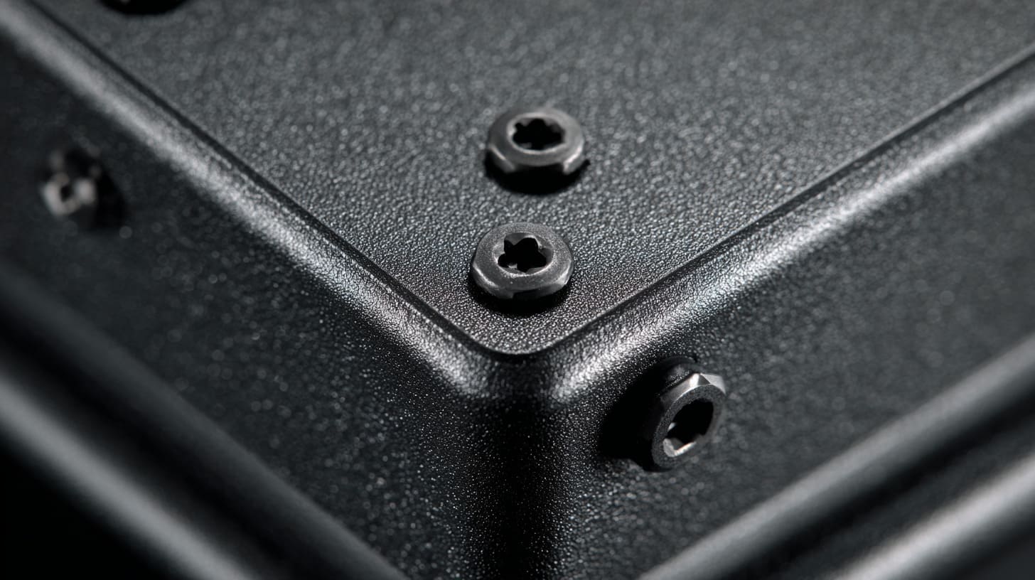
This is the heart of the problem.
When the mating surfaces are fully anodized, the parts may still fit together well. The lid may sit flat. The joint may look premium. The screws may tighten without any drama. But electrical continuity across the seam can be weak, unstable, or missing.
That is why full anodizing creates EMC risk. Not because anodizing is bad in general. It is because the wrong surface condition is placed in the wrong location.
Insulating layer blocks electrical continuity
The anodized layer acts like a barrier between two metal parts. So even when those parts are pressed together, the conductive path is not what many engineers assume.
That raises contact resistance. In some cases, the path becomes inconsistent. In other cases, it becomes so weak that the seam behaves more like a break than a connection.
I have seen samples where the enclosure looked excellent and still felt electrically suspicious the moment I reviewed the contact zones. That feeling usually comes from experience, not theory. A seam that is too perfect in color often makes me ask one quiet question: where is the actual metal-to-metal path?
Formation of unintended gaps
A tight mechanical fit is not the same as a good electrical fit. That sentence has saved me from more than one bad assumption.
People often trust what they can see:
- no visible gap
- no loose corner
- no movement in the lid
- no assembly issue
But EMC does not care about that visual comfort. If the contact surfaces are insulated, the electrical path is still broken. Tiny discontinuities can behave like leakage points. And at high frequencies, even small problems can become loud ones.
High-frequency behavior makes the issue worse
At higher frequencies, current prefers to move along surfaces. That means enclosure seams become even more important. A weak seam can interrupt surface current flow, increase emissions, or reduce shielding effectiveness.
The effect is not always obvious in early prototype handling. The part feels strong. The sample looks mature. Then the product enters test, and the seam starts telling the truth.
| Full anodized mating surface effect | What it looks like in assembly | What it can cause in EMC |
|---|---|---|
| Oxide barrier between parts | Clean premium finish | Poor continuity |
| Higher contact resistance | No visible issue | Weak shielding path |
| Inconsistent seam conduction | Unit seems normal | Variable test results |
| Surface current disruption | Good cosmetic quality | Radiated emission risk |
I do not call a design safe just because it feels well-machined in the hand. If the electrical path depends on hope, the enclosure is not ready.
And once that risk enters real products, it does not stay polite. It shows up in failure modes that waste time, money, and patience.
Real-World Failure Modes Caused by Anodized Mating Surfaces
The hardest part about this problem is that it often stays quiet until the wrong moment.
A drawing review may not catch it. A quick sample inspection may not catch it. Even assembly may feel smooth. Then testing starts, or field use begins, and the nice-looking enclosure suddenly becomes a project problem.
I have seen that pattern enough times that I no longer call it rare.
EMC test failures
The first place this issue often becomes visible is EMC testing.
A product may show:
- radiated emissions above limit
- unstable results between repeated tests
- unexpected sensitivity in noisy environments
- poor shielding performance around seams
The frustrating part is that teams often start blaming the board first. That is understandable. The board is active, complex, and full of components. But sometimes the quiet offender is the seam with no real conductive path.
Unstable grounding and bonding
Another problem is inconsistency. One sample seems acceptable. Another one is worse. A third one passes until vibration, reassembly, or slight process variation changes the contact quality.
That kind of instability is dangerous because it confuses people. A fixed design should behave in a stable way. When the bonding path depends on random pressure, screw behavior, or local coating damage, the design is not robust.
I get cautious anytime the only “bonding solution” is a screw pressing through finished surfaces and hoping for enough contact. That is not engineering confidence. That is borrowed luck.
Field performance issues
Even when a product survives lab work, bad mating surface design can still create field problems.
Possible issues include:
| Field issue | How it shows up | Why it hurts the business |
|---|---|---|
| Interference with nearby devices | Noise complaints, unstable operation | Damages product reputation |
| Unit-to-unit inconsistency | Some units behave worse than others | Creates support headaches |
| Delayed certification | More test rounds and redesigns | Slows launch and raises cost |
| Rework at production stage | Extra masking, grinding, patch fixes | Reduces margin and speed |
I remember one style of project where the outside finish looked so good that everyone wanted to keep it untouched everywhere. The team delayed dealing with the contact zones because nobody wanted to “spoil” the look. Later, the test failure spoiled a lot more than the look. It spoiled the schedule.
A hidden surface problem can create very public delays. And that leads to another mistake I see often: trusting screws to fix what the surface finish already broke.
Why Screws Alone Cannot Solve the Problem
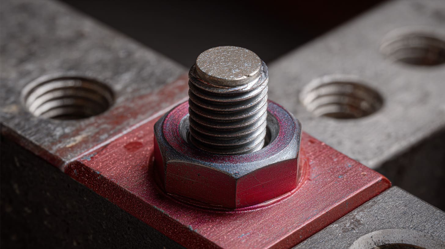
A screw can hold parts together very well. I respect screws for that. But I do not trust them blindly for EMC bonding.
That difference matters.
Many teams see a tight screw and feel safe. The joint feels firm. The assembly feels finished. The housing looks solid in the hand. I understand why that creates confidence. Still, mechanical clamping and electrical bonding are not the same job.
Mechanical fastening vs electrical bonding
A screw provides force. It pulls surfaces together. That is valuable. But conductivity depends on what sits between those surfaces.
If the mating area is fully anodized, then the screw is tightening insulated surfaces together. The screw may create a tiny local contact point somewhere. It may even scratch through the finish in one place. But that is not the same as designing a stable conductive path.
I judge screw-based bonding with extra suspicion when the design seems to rely on “probably enough contact.” That phrase has a bad history in enclosure work.
Surface oxidation and coatings reduce contact
The screw head area can also be misleading. People assume the screw connection solves everything. But the anodized layer remains under much of the contact area. The actual conductive zone may be tiny, uneven, or unstable.
Common issues include:
- coating remains under the head
- contact area is small
- pressure is not evenly distributed
- local damage creates unpredictable conductivity
- repeated assembly changes the result
Long-term reliability concerns
Even if the screw contact seems acceptable at first, long-term behavior can still go wrong.
Vibration, handling, oxidation, thermal cycling, and repeated opening of the enclosure can all change the contact quality over time. That is why I do not like turning a screw into the hero of an EMC strategy. It has too many ways to disappoint.
| Screw-related assumption | Reality I usually see |
|---|---|
| “The screw makes it conductive” | Sometimes only in a weak, local, or unstable way |
| “Tight assembly means safe bonding” | Tightness does not prove low impedance path |
| “It passed once, so it is fine” | One pass does not prove production reliability |
| “More screws will fix it” | More weak contacts do not always create one strong path |
I have no problem using screws in an EMC design. I just do not want them doing a job they were never clearly designed to do on their own.
Once that sinks in, the conversation gets more useful. We stop hoping the joint will save us, and we start designing the bonding path on purpose.
Design Strategies to Avoid EMC Risk
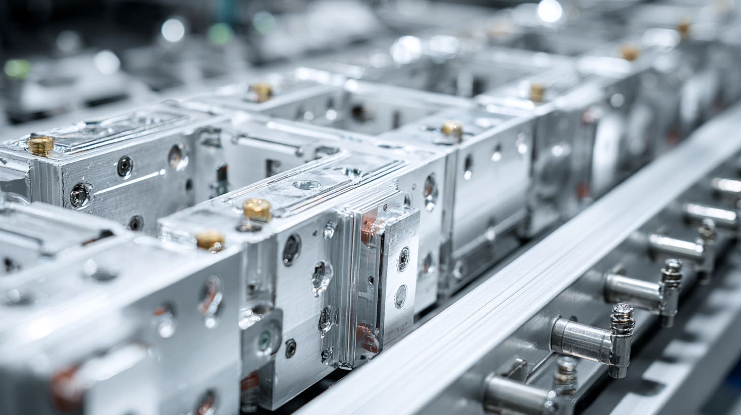
This problem is avoidable. That is the good news.
I do not say that lightly. Some EMC issues are messy and hard to isolate. This one is often more manageable if the team respects it early enough. The key is simple: design the conductive path on purpose instead of treating it like a lucky side effect of assembly.
Masking mating surfaces during anodizing
One of the most common and practical solutions is masking the mating surfaces before anodizing. That keeps key contact zones free from the insulating anodized layer.
This approach gives me a good balance in many projects:
- visible surfaces still get the premium anodized look
- contact areas stay conductive
- bonding across seams becomes more reliable
- the design keeps both beauty and function in view
When I review a custom enclosure with EMC needs, I often pay close attention to which surfaces deserve finish and which surfaces deserve honesty. Not every area should be treated the same.
Adding dedicated grounding points
A dedicated grounding point is much better than vague hope.
This may include:
- grounding studs
- conductive inserts
- bare contact pads
- serrated washers
- star washers
- defined bonding hardware
These solutions create intentional contact paths. I like that because intentional design is easier to explain, inspect, and repeat in production.
Using conductive gaskets or EMI materials
For some projects, conductive gaskets or EMI shielding materials help a lot. They can improve seam continuity and reduce leakage through small gaps.
They are not always the cheapest path, and they are not always needed. Still, when the enclosure shape, frequency range, or sealing need gets tougher, they become very useful.
Designing clear bonding paths from the start
This is the part I value most. I want the electrical path to be obvious in the design. I do not want to hunt for it after the enclosure is built.
Here is a simple planning view:
| Strategy | Cost impact | EMC benefit | My view |
|---|---|---|---|
| Masking contact areas | Low to medium | High | Often the smartest first move |
| Dedicated grounding points | Medium | High | Good for robust designs |
| Conductive gasket | Medium to high | High | Strong option for critical seams |
| Rely on screws only | Low at first | Uncertain | Often becomes expensive later |
The smartest enclosure teams I work with do not leave bonding to chance. They decide where current should flow, how seams should behave, and what production needs to protect.
That kind of planning sounds simple. It is simple. But it asks for discipline. And discipline always meets the same old engineering question: what are we willing to trade for appearance, corrosion resistance, and cost?
Trade-Off Between Corrosion Resistance and EMC Performance
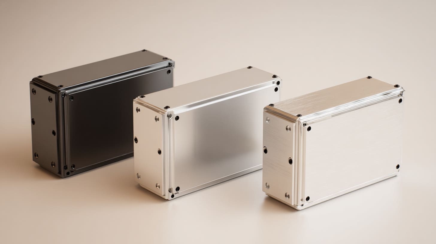
This is where the conversation gets honest.
Full anodizing has real value. I use it. I recommend it. I sell projects that need it. I am not against it. But I do not like one-sided thinking. A finish that helps corrosion resistance can create EMC trouble. A finish that looks complete can leave the enclosure electrically incomplete.
That tension is normal. The key is to respect it.
Benefits of full anodizing
There are clear reasons buyers and engineers like full anodizing:
- uniform appearance
- strong corrosion resistance
- better wear performance
- cleaner product image
- easier brand positioning for premium products
For some products, those gains matter a lot. Outdoor use, long service life, and strong visual requirements can all push the design toward more surface protection.
Risks introduced by full anodizing
The risk starts when people assume those benefits come with no trade-off.
They do not.
Once the mating surfaces are fully anodized, the design can lose:
- reliable electrical continuity
- stable seam conductivity
- predictable EMC behavior
- easy bonding through ordinary contact zones
I usually slow the team down at this point and ask what hurts more: a controlled visible bare contact zone, or an expensive EMC problem hiding under a perfect finish? That question often changes the mood in the room.
A balanced approach usually works better
In many real projects, the best answer is not “anodize everything” or “leave everything raw.” The best answer is selective treatment.
That may mean:
- anodize visible outer faces
- mask mating surfaces
- protect critical contact areas in another way
- combine finish strategy with bonding hardware
- adjust design based on environment and EMC level
| Design choice | Appearance | Corrosion resistance | EMC confidence |
|---|---|---|---|
| Full anodizing everywhere | Excellent | Excellent | Lower on mating surfaces |
| Bare aluminum everywhere | Weak to moderate | Lower | Better conductivity, weaker protection |
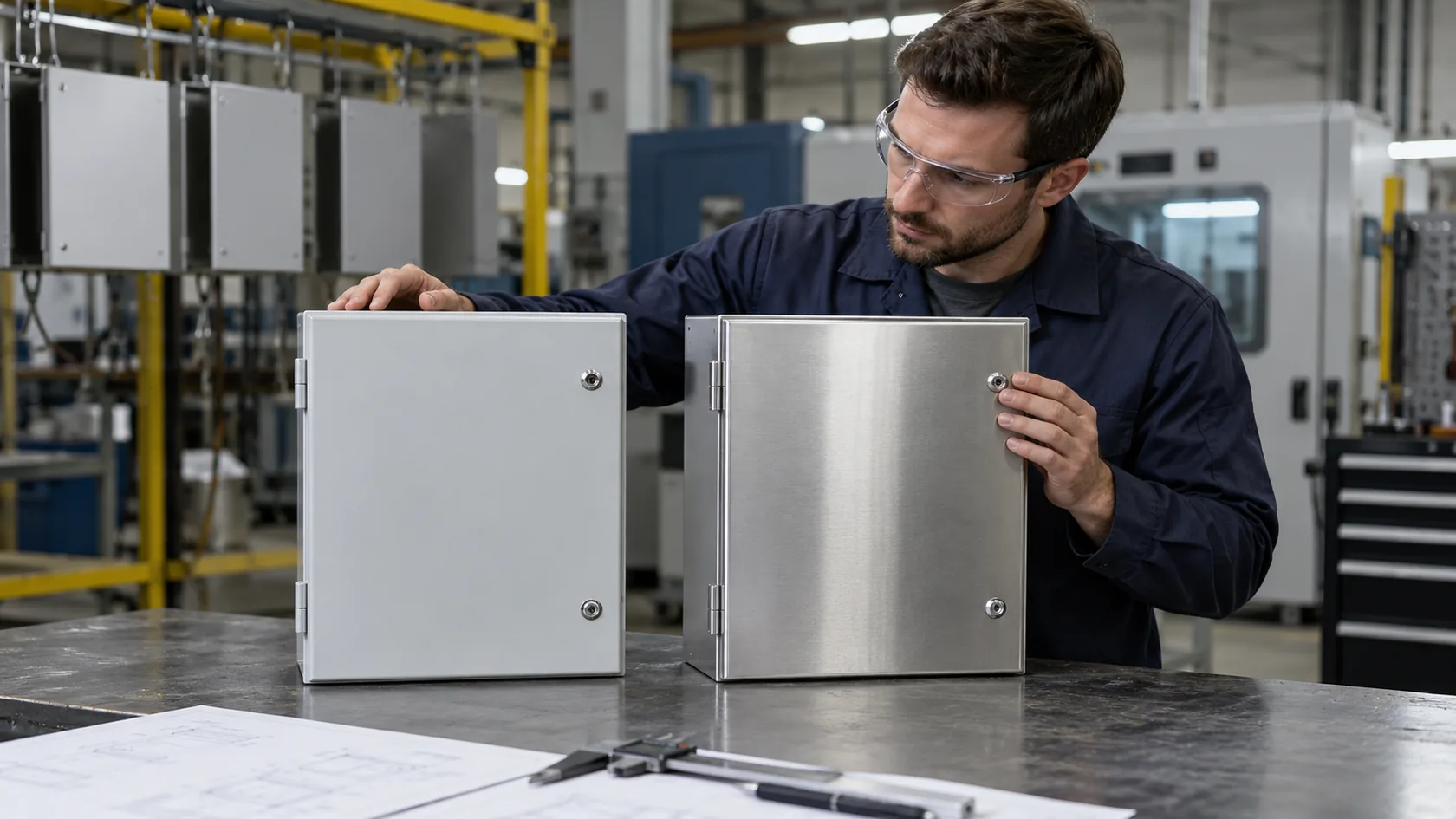
| Selective anodizing | Very good | Very good | Usually the best balance |
I rarely believe the best design is “fully treated everywhere.” Real engineering usually asks for more nuance than that. The surface should match the job, not the mood.
And once that trade-off is clear, it becomes easier to understand why experienced engineers handle this issue differently from teams learning it the hard way.
How Experienced Engineers Handle This Issue

Experience changes the questions people ask.
Less experienced teams often ask, “Does this enclosure look good?” or “Can we anodize the whole part?” Those are not bad questions. They are just incomplete. Experienced engineers usually ask something else first: “Where is the conductive path?” That one question saves a lot of trouble.
I have learned to respect early questions more than late heroics.
Early-stage design decisions
The best results usually start before the first sample.
Good teams define:
- EMC level needed
- key bonding paths
- seam sensitivity
- finish requirements by zone
- which surfaces must stay conductive
That early clarity matters because it prevents surface treatment from becoming a surprise later.
Collaboration between teams matters
EMC problems often grow in the space between departments.
The mechanical team may choose finish based on durability and appearance. The electrical team may assume continuity exists. The supplier may follow the drawing exactly. Everyone can be reasonable, and the product can still fail.
That is why I like direct conversations between mechanical, electrical, and manufacturing people. Not long dramatic meetings. Just honest coordination early enough to matter.
I trust a project more when the enclosure supplier is brought into the surface treatment discussion before production, not after a failed test report lands on the table.
Prototype and validation strategy
The smartest teams test before they are forced to.
That may include:
- continuity checks at seams
- bonding resistance checks
- pre-compliance EMC testing
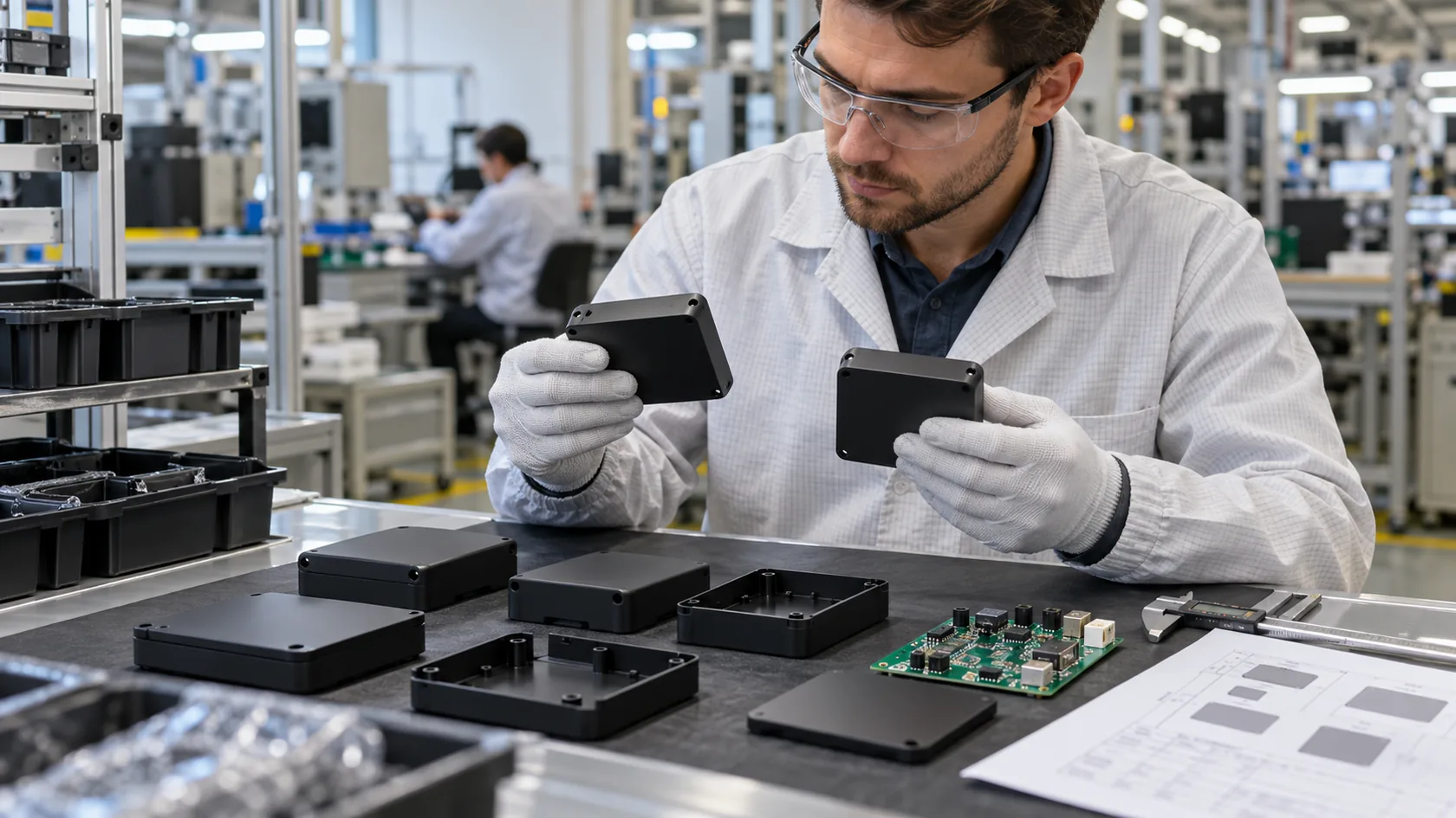
- comparison of masked vs fully anodized samples
- repeated assembly checks
| Team habit | Weak project behavior | Strong project behavior |
|---|---|---|
| Surface treatment review | Chosen only by appearance | Chosen by function and appearance |
| EMC thinking | Starts after failure | Starts during enclosure design |
| Supplier communication | Basic drawing transfer | Detail discussion on contact zones |
| Prototype strategy | One “nice” sample | Functional sample with validation intent |
I have noticed that experienced engineers do not panic less because they are smarter by nature. They panic less because they leave fewer silent assumptions inside the product.
That is the real advantage. Not genius. Just fewer blind spots.
Conclusion
I believe full anodizing on mating surfaces creates EMC risk because I have seen how easy it is for people to trust what looks finished. A premium enclosure can make a team feel safe before the electrical path has earned that trust. That is the core problem for me.
I think this way because I do not separate finish decisions from system behavior. The surface is not just color. It is not just corrosion resistance. It is part of how the enclosure performs in the real world. Once I learned that the hard way through real projects, I stopped treating anodizing like a harmless last step.
My view comes from a simple pattern I have seen again and again. A project looks clean. The assembly feels solid. The screws are tight. The sample photographs well. Then EMC testing exposes what the eye could not see. The seam was never truly acting like one conductive structure. The product looked complete, but the shielding path was incomplete.
That is why I usually push for selective thinking. I want the visible areas to look good. I want the enclosure to resist wear and corrosion. But I also want the contact zones to behave honestly. I would rather explain a masked mating surface early than explain a failed EMC result late.
For me, the real lesson is not “do not use anodizing.” The real lesson is “do not use it everywhere without asking what that surface must do.” That small question saves money, time, and painful redesigns.
If you are working on a custom aluminum enclosure and EMC matters for your product, send me your drawing or your rough idea. I can help you review the mating surfaces, the finish strategy, and the bonding path before those hidden risks become expensive problems.