Skip to content
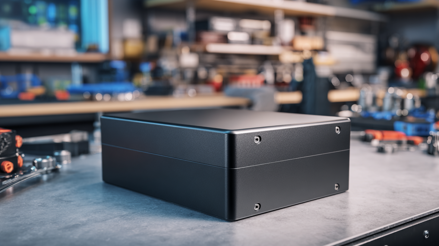
A neat aluminum enclosure can fool people very fast.
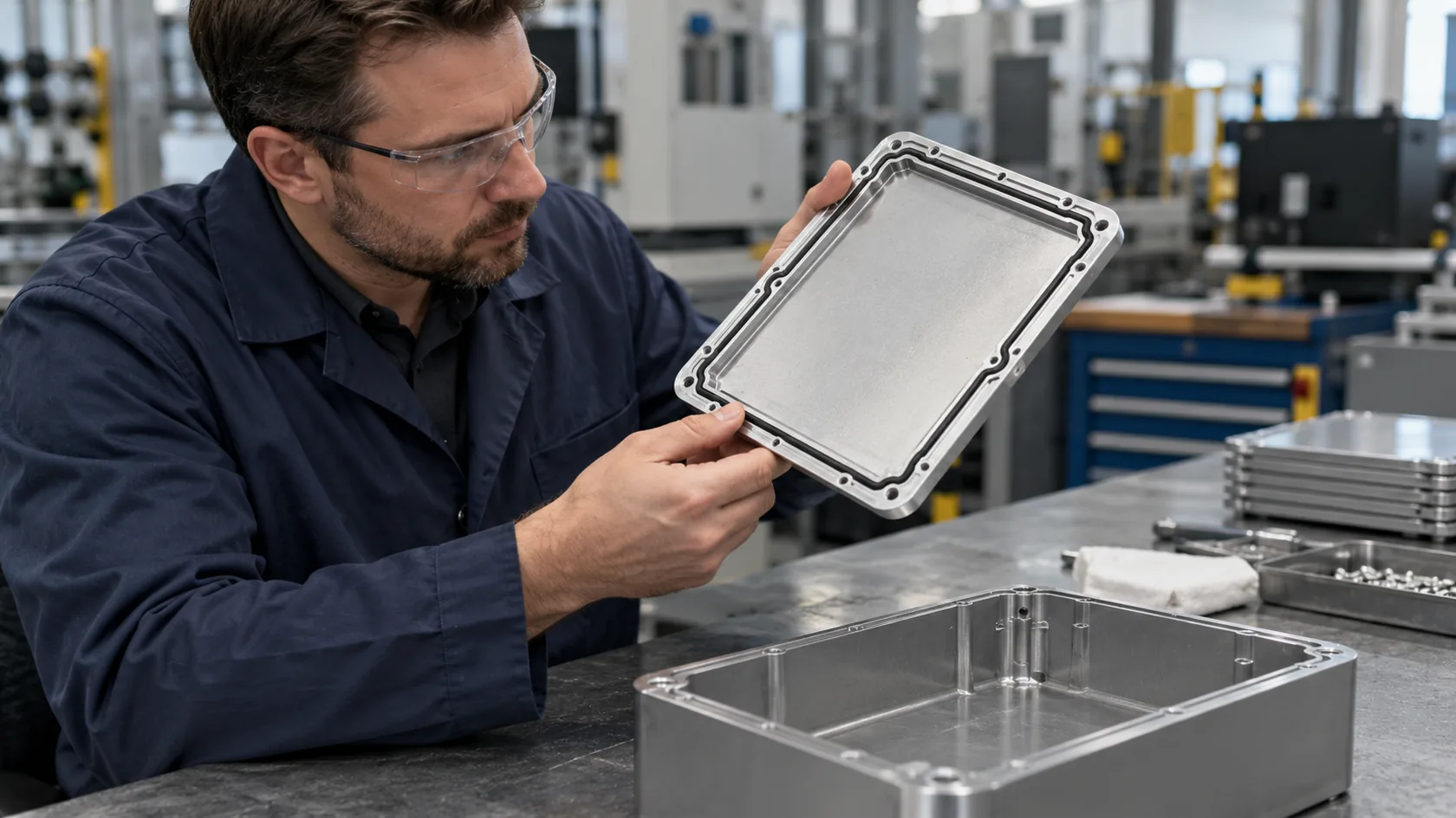
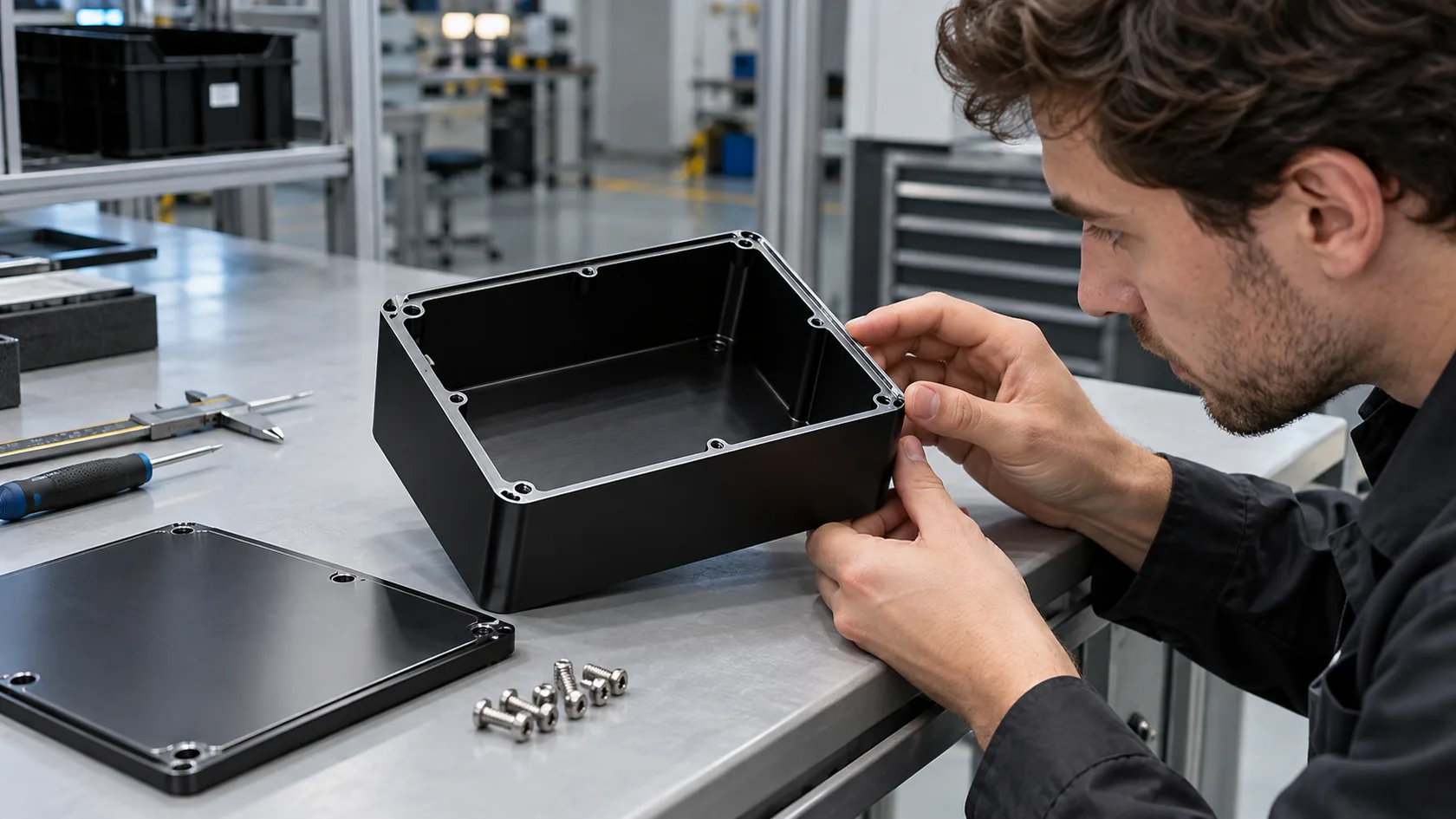
The edges are sharp. The finish looks premium. The color feels clean and controlled. A black anodized case on a bench often sends the same signal: this product is already under control. I understand that reaction because I have had it too. Good anodizing makes an enclosure look serious. It also helps with corrosion resistance, wear, and brand image. For many industrial products, that matters a lot.
But this is also where the quiet trouble begins.
I have seen enclosures that looked excellent in sample photos and still caused real headaches later. The machining was fine. The logo position was right. The fit between top and bottom covers looked tight. Then the product went into EMC testing, and the result made everyone uncomfortable. The problem was not the board layout people were staring at all week. The problem was the seam.
That gap between looks conductive and actually works electrically catches many engineers.
EMC is one of those topics that pushes teams into blame mode very quickly. The hardware engineer points at the PCB. The PCB designer points at the cable. The enclosure supplier gets pulled in later. Then someone notices the anodized mating faces, the coated screw areas, or the long untreated seam, and the whole story changes.
What pushes me to this conclusion is simple: when I see a failed EMC result in an anodized aluminum product, I do not start by admiring the schematic. I start by asking where the current is supposed to cross the housing, and whether the enclosure is secretly open in the one place that matters.
A lot of EMC trouble starts there.
And once I learned to look at seams before traces, many “mysterious” failures stopped feeling mysterious at all.
What Is EMC and Why Does It Fail in Real Products?

EMC sounds technical and distant when people first hear it. In real work, it is much more practical than that. EMC is just the question of whether a product can live in the real electrical world without making too much noise or getting pushed around by the noise around it.
That sounds simple. It is not.
What EMC actually means in practice
EMC usually gets split into two parts:
| Part | What it means | What can go wrong |
|---|---|---|
| Emissions | The product sends out unwanted electrical noise | The device disturbs nearby equipment |
| Immunity | The product resists outside electrical noise | The device resets, malfunctions, or becomes unstable |
A product can have a smart PCB and still fail both sides. That is the part many teams do not like to hear. EMC is not only a board problem. It is a full-system problem.
I have seen engineers spend days tuning filters, ferrites, and ground pours while the enclosure was quietly leaking energy through a seam like a half-open zipper.
Why EMC failures are often surprising
A product can look stable in the office and fail badly in the lab. That gap surprises people because the prototype often appears normal during ordinary use.
Here is why EMC failures catch teams off guard:
- The product still powers on
- The signals still look fine at low-speed checks
- The housing still feels solid in the hand
- The failure only appears under specific test conditions
- The actual root cause may be mechanical, not schematic
That last point matters a lot.
Small mechanical details can create large electrical effects. A tiny break in continuity at a seam may look harmless to the eye. At higher frequencies, it can behave like an open door.
Why engineers often blame the PCB first
I understand why this happens. The PCB is visible. It has traces, planes, filters, chips, and test points. Engineers can zoom in on it. They can change it. They can discuss it in meetings for hours.
The enclosure is different. It feels passive. It looks like the quiet part of the system. It gets treated like a shell.
That is often the mistake.
| Why the PCB gets blamed first | Why that can be misleading |
|---|---|
| It is easier to analyze | The enclosure affects current return paths too |
| It contains the electronics | The housing can become part of the RF behavior |
| It has obvious design features | Seams and coatings are easy to overlook |
| It feels more “electrical” | EMC failures often come from mechanical-electrical interaction |
I do not say the PCB is unimportant. Of course it matters. A noisy board can cause real trouble. But I do not trust the common habit of blaming the board first, because that habit is comfortable, and comfortable habits often waste the most time.
That is where the metal box enters the story in a much bigger way than people expect.
How Enclosures Influence EMC Performance
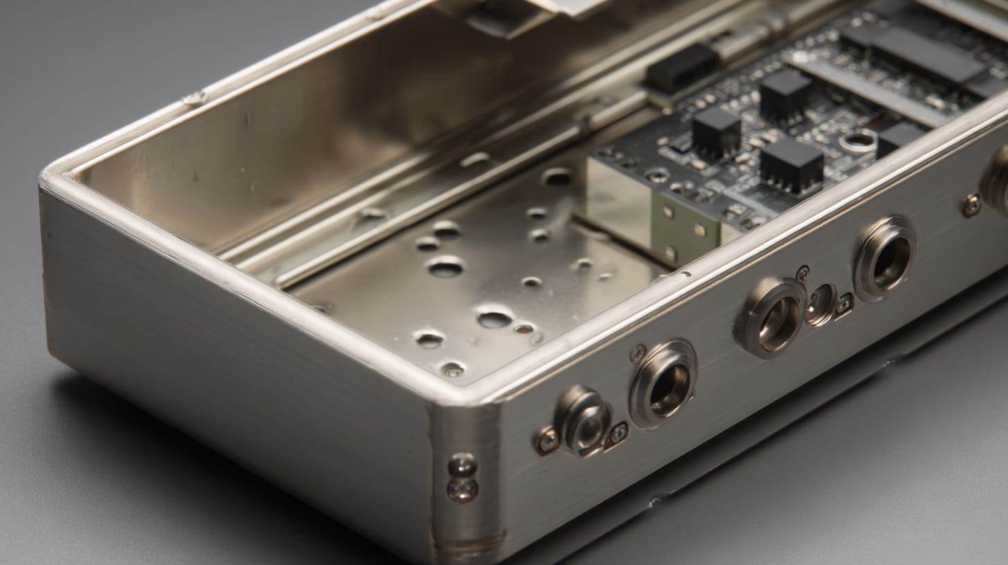
An enclosure is not just a package. It is not just there to protect the board from dust, fingers, impact, or weather. In many products, the enclosure is also part of the EMC design whether the team planned for that or not.
That is why a beautiful case can become an ugly surprise.
Enclosure as a Faraday cage
When people talk about a metal enclosure helping EMC, they usually mean the housing acts like a shield. That idea comes from the Faraday cage concept. The metal body surrounds the electronics and helps contain or block electromagnetic energy.
But that only works well when the shield is continuous.
A metal box with poor electrical joints is like an umbrella with holes in it. It still looks like protection. It just stops protecting where the problem starts.
The role of seams and joints
Every seam in a metal enclosure is a weak point. Some seams are small and well controlled. Some are long, loose, or coated. Some are pressed together well in CAD, but not well in production.
That difference matters.
High-frequency current does not move through a product in the simple, slow way many people imagine. It tends to flow along surfaces. It follows the path that makes the most electrical sense at that frequency. If the seam interrupts that path, current does not politely disappear. It reroutes.
And when it reroutes badly, the product radiates.
Contact resistance and current flow
Good shielding needs good contact. That means low and stable resistance across mating parts. If the resistance is too high or too inconsistent, the seam stops acting like a solid conductive boundary.
Here is a simple way I look at it:
| Seam condition | What it usually means for EMC |
|---|---|
| Clean metal-to-metal contact | Better shielding continuity |
| Painted or anodized mating surface | Poor continuity |
| Loose mechanical pressure | Unstable contact |
| Long seam with few bonding points | More leakage risk |
| Corroded or oxidized contact point | Higher resistance over time |
This is why I do not let myself get impressed too quickly by a box that merely looks closed. A housing can be mechanically closed and electrically open at the same time, and that difference is exactly where a lot of EMC pain begins.
The next step is the surface itself, because anodizing changes the whole behavior of aluminum in a way many teams underestimate.
What Is Anodizing and Why It Changes Everything
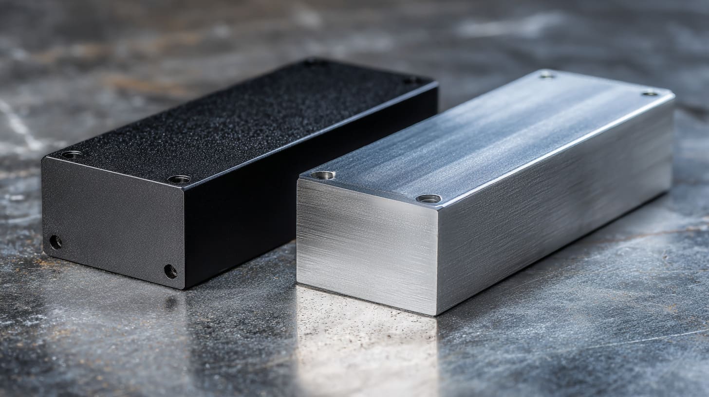
I like anodizing. I use it often. Many customers want it, and for good reasons. It gives aluminum a cleaner look. It improves corrosion resistance. It makes products feel more finished. It can also help a brand look more serious in the market.
Still, I never treat anodizing like a purely cosmetic choice.
Basics of anodized aluminum
Anodizing creates an oxide layer on the aluminum surface. This layer is harder than raw aluminum and much better for appearance and corrosion control.
That sounds like a win. In many ways, it is.
For enclosure projects, anodizing gives several benefits:
- Better surface finish
- More stable appearance
- Better resistance to wear
- Better resistance to corrosion
- More color options
- Stronger visual value for the product
That is why so many teams choose it.
Electrical properties of anodized surfaces
Here is the part people forget: anodizing creates an insulating layer.
That means the surface no longer behaves like bare conductive aluminum. So if two anodized parts touch each other at the seam, they may not create the electrical path the EMC design needs.
This is not a small side note. This is the whole issue.
| Surface type | Conductive behavior |
|---|---|
| Bare aluminum | Conductive, though oxide still matters |
| Anodized aluminum | Surface is largely insulating |
| Painted aluminum | Surface is insulating |
| Powder-coated aluminum | Surface is insulating |
That table looks basic, but it saves real projects.
I have seen teams choose anodizing for good commercial reasons and then act surprised when the housing stops helping EMC. The surprise itself is the problem. The surface changed. The electrical behavior changed too. That should never be treated as separate.
Thickness and uniformity of anodizing
Many anodized layers are not visually dramatic. They can be thin and still create a real electrical break. Typical anodizing thickness may fall around 5 to 25 microns depending on the process and purpose. That sounds tiny. For EMC contact paths, tiny is enough.
Even a thin layer can stop reliable metal-to-metal conduction.
That is why I do not judge anodized contact areas by eye. A surface can look harmless and still behave like a wall. The premium look is useful, yes, but electrically it can turn a nice aluminum enclosure into a set of separated metal pieces pretending to be one shield.
And that is exactly why the seam becomes the next place I look.
Why EMC Problems Often Start at the Anodized Seam
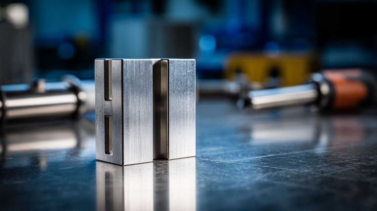
This is the center of the whole article.
A lot of EMC problems do not begin at the chip, the trace, or the filter. They begin where two anodized metal parts meet and quietly fail to conduct.
Loss of electrical continuity at seams
When mating faces are anodized, they often stop providing reliable conductive contact. The parts still bolt together. The seam still looks neat. But the electrical path across that joint can be weak, unstable, or missing.
That changes the enclosure from one conductive body into several separate pieces.
And separated pieces do strange things during EMC testing.
- One part may float electrically
- Current may search for a new path
- Noise may couple into unexpected areas
- The shield loses continuity
- Emissions rise for reasons that seem unrelated at first
I have watched teams chase PCB fixes for days while the real problem sat in the housing seam the whole time.
Seams acting as slot antennas
A narrow seam can act like a slot antenna. That phrase sounds dramatic, but the idea is simple. A small opening in a conductive structure can let energy leak out, especially at higher frequencies.
The risk grows when:
- The seam is long
- Contact is poor
- Bonding points are too few
- Mechanical pressure is uneven
- The opening sits near noisy internal sources
High-frequency current interruption
At high frequencies, current follows the surface. That is one reason enclosure continuity matters so much. If the current reaches an anodized seam and cannot cross cleanly, it does not just stop and accept its fate. It finds another route.
That rerouting often creates larger current loops or pushes energy into places where radiation gets worse.
| Seam behavior | Likely EMC effect |
|---|---|
| Continuous conductive seam | Better containment |
| Interrupted seam | Current rerouting |
| Long insulating seam | More leakage risk |
| Inconsistent contact | Unstable test results |
When I see this in real work, I do not think of it as a “small contact issue.” I think of it as a broken road in the exact place where the traffic needed to pass.
Real-world failure patterns
Some EMC failures have a pattern that becomes obvious once you have seen it enough times.
A product has:
- A decent PCB layout
- Sensible grounding on the board
- Good filtering effort
- A metal enclosure
- A premium anodized finish
- Poor seam continuity
Then the product fails.
Then someone removes coating at the bonding point, adds conductive gasketing, or changes the seam contact strategy, and the result improves much more than expected.
That kind of result teaches a blunt lesson. If current cannot cross the seam, it will escape somewhere else, and the product will pay for that escape in the test lab.
Once I learned that lesson, I started seeing another issue again and again: engineers trusting mechanical assembly details that do not deserve that trust.
Common Design Mistakes Engineers Make
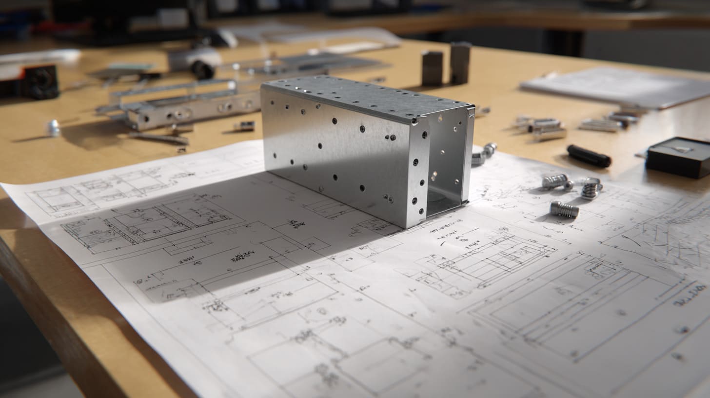
Most EMC mistakes around anodized enclosures are not dramatic. They are ordinary. That is why they survive so long in projects. They hide inside assumptions that sound reasonable at first.
Assuming screws provide sufficient grounding
This is one of the most common mistakes.
A screw can clamp two parts together. That does not automatically mean it creates a low-impedance electrical bond across the seam. The contact area is small. The pressure may vary. The coating may remain in the way. The result may work in one unit and fail in another.
I have seen products where the team basically hoped the screws would “take care of it.” Hope is not a bonding method.
| Assumption | Reality |
|---|---|
| Screws always bond the seam | Often false |
| Tightening harder solves it | Not always |
| Mechanical contact means electrical contact | Not the same thing |
| One screw point is enough | Often risky |
Ignoring coating impact during design
Some teams design the enclosure as if aluminum is simply aluminum. They forget that the final surface treatment changes the electrical story.
That leads to problems like these:
- No masked contact area
- No dedicated bonding pad
- No EMI gasket plan
- No continuity check after finishing
- No seam strategy in the drawing stage
This is where things often go bad in a very quiet way. The design looks complete. The finish is approved. The parts arrive. Then the housing behaves nothing like the team imagined.
Over-reliance on PCB shielding techniques
I respect good PCB EMC design a lot. I also know its limits.
Ferrites, filters, shield cans, and clean ground layout are valuable. But they cannot fully compensate for an enclosure that leaks through an anodized seam. If the box is open electrically, the board is being asked to solve a housing problem, and that is unfair to the board.
Designing seams too long or poorly aligned
Long seams create more chance for leakage. Poor alignment makes contact less stable. Low screw count spreads bonding points too far apart. Decorative priorities can also work against EMC.
I have seen products where the seam looked elegant in CAD but acted like a broadcast line in testing.
Here is a quick view:
| Design mistake | Why it hurts |
|---|---|
| Long seam length | More leakage opportunity |
| Few fastening points | Less consistent contact |
| Poor alignment | Uneven pressure |
| Decorative finish over all contact zones | No conductive path |
| No bonding feature in the design | Late-stage EMC trouble |
A box that assembles nicely is not automatically a box that bonds well. I have learned to separate those two ideas every single time.
That is why real design work needs a more intentional approach.
How to Properly Design Around Anodized Seams
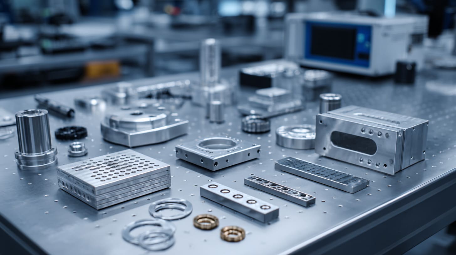
Once a team accepts that anodized seams are part of the EMC problem, the good news is that practical fixes exist. These fixes are not magic. They are mostly about being deliberate early enough.
Masking critical contact areas
One of the most useful methods is selective masking. That means leaving certain seam contact areas free of anodizing so the metal parts can touch each other directly.
This can be done at:
- Screw bonding zones
- Mating flanges
- Ground points
- EMI gasket contact areas
- Dedicated continuity bridges
I tend to trust masked contact areas far more than random pressure through coated parts, because random contact may pass once and fail later.
Using conductive gaskets and EMI seals
When the seam design needs stronger EMC control, conductive gasketing helps a lot. These materials create electrical continuity while also helping seal the gap.
Common options include:
| Material | Typical use | Notes |
|---|---|---|
| Conductive foam | Light contact seams | Flexible, easy to use |
| Conductive fabric over foam | General EMI sealing | Good for many enclosure types |
| Beryllium copper finger stock | Strong spring contact | Effective, but needs proper design |
| Conductive elastomer | Sealing + conductivity | Useful in specific environments |
The right choice depends on cost, compression, life cycle, corrosion risk, and assembly method.
Designing dedicated bonding paths
I prefer dedicated bonding paths over accidental ones.
That means the design should show clearly where current is supposed to cross from one enclosure part to another. That can include:
- Ground straps
- Copper braid
- Bonding tabs
- Dedicated bare metal pads
- Multi-point seam bridges
When I look at a housing drawing, I want to see that path in my head without guessing. If I cannot see it clearly, I assume the lab may expose the weakness later.
Optimizing screw and fastening strategy
Screws can still help. They just should not carry the whole burden alone.
A better fastening strategy may include:
- More evenly spaced fasteners
- Star washers to cut through surface films
- Controlled torque
- Shorter distance between bonding points
- Washer and pad design that supports real contact
| Fastening detail | Better approach |
|---|---|
| Decorative screw placement | Functional bonding placement |
| Random torque | Controlled torque |
| Smooth washer only | Star washer where appropriate |
| Few screw points | Better-distributed pressure |
I have found that good EMC results usually come from intentional current paths, not from lucky metal contact that happened to work in one sample.
Of course, design intent still needs proof. That proof comes from testing.
Testing and Verifying Seam Performance

One reason seam problems survive too long is simple: teams do not always measure them directly. They inspect the parts visually. They tighten the screws. They assume the connection exists.
I do not like that kind of assumption anymore.
Measuring contact resistance
A seam should be checked electrically, not just mechanically. Low-resistance measurement between enclosure sections can reveal whether the intended bond is actually there.
This does not need to be mysterious. The goal is to check whether the connection is:
- Low enough
- Stable enough
- Repeatable enough
- Present in real assembly condition
A clean-looking seam tells me almost nothing by itself. I would rather see one honest resistance reading than ten confident opinions around a meeting table.
Pre-compliance EMC testing
Pre-compliance work saves pain. It helps the team catch leakage paths before the expensive formal test stage.
Useful checks include:
- Near-field probing around seams
- Comparing coated vs masked seam versions
- Testing with and without conductive gasketing
- Watching emission changes after seam modifications
- Checking different torque conditions
That kind of testing often shows the truth very fast.
Visual vs electrical inspection
This is one of the biggest mindset shifts I try to push in enclosure work. A clean seam is not the same as a good seam. A premium finish is not the same as a bonded finish.
| Inspection type | What it can miss |
|---|---|
| Visual check | Hidden electrical isolation |
| Mechanical fit check | High contact resistance |
| Cosmetic approval | Poor EMC continuity |
| Basic assembly review | Weak seam current path |
If I cannot measure the connection, I do not trust it, especially on anodized aluminum. That may sound cautious, but failed EMC projects are expensive teachers, and I do not enjoy paying them twice.
Once testing makes the issue visible, the final question becomes practical: what solutions are worth using in real industry work?
Practical Solutions Used in Industry
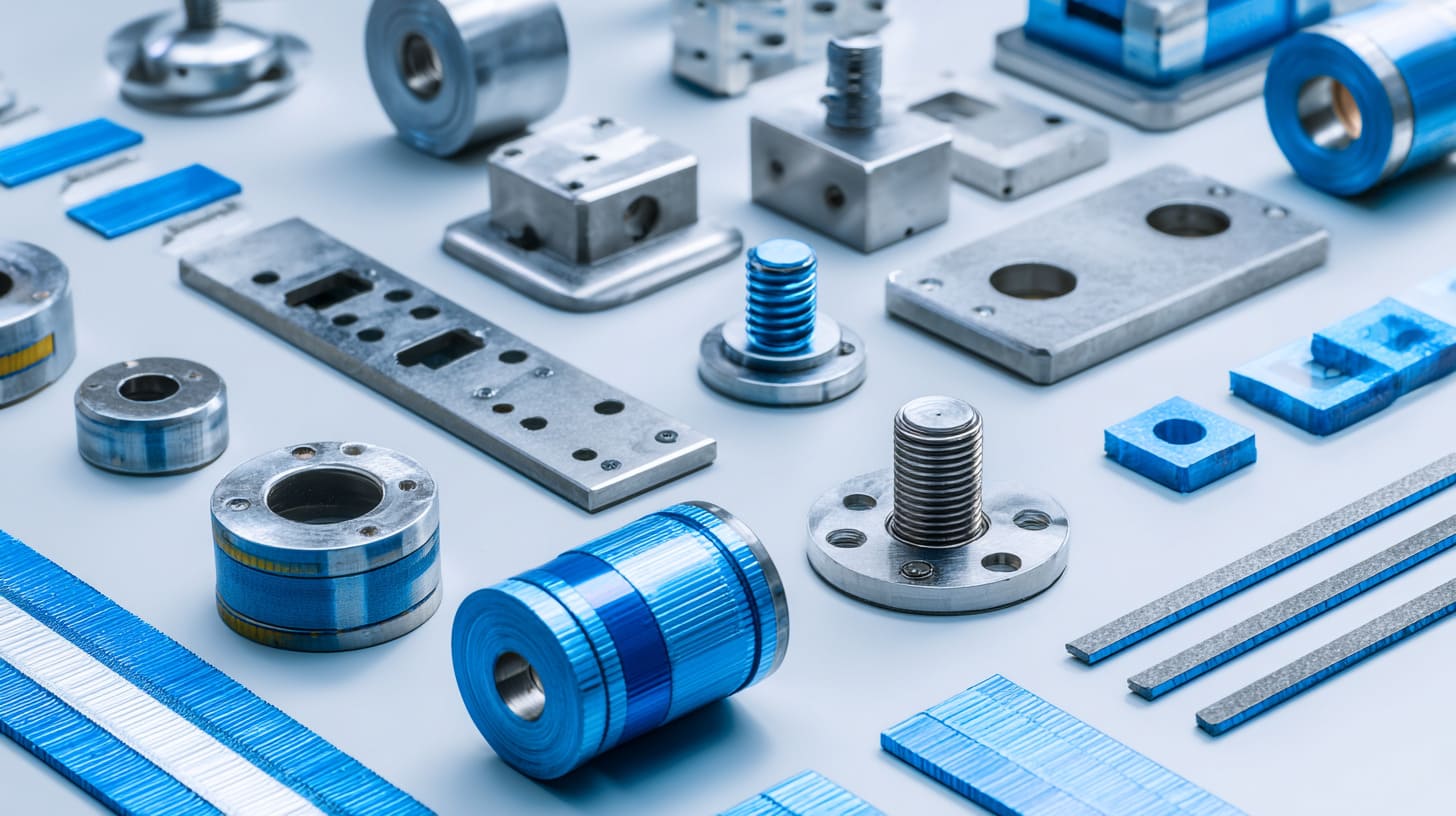
Real projects do not live inside theory alone. They live inside budgets, lead times, customer expectations, surface finish demands, and factory limits. That is why the best EMC solution is not always the most elegant one on paper. It is the one that works, can be repeated, and makes business sense.
Hybrid surface treatments
Many teams do not want to give up anodizing, and I do not blame them. The finish has real value. So the practical answer is often not “remove anodizing everywhere.” It is “use anodizing more intelligently.”
That can mean:
- Anodize visible exterior areas
- Mask seam bonding zones
- Leave specific grounding pads bare
- Combine appearance control with electrical planning
This balance is often the smartest move. It protects the brand look without sacrificing function.
Modular enclosure bonding design
Some enclosure designs handle EMC better because they were built around seam control from the beginning. The bonding points are planned. The pressure is distributed. The seam is short or segmented. The current path is obvious.
That type of design usually feels less dramatic during certification, and I say that as a compliment.
Cost vs performance trade-offs
This part matters for buyers and engineers alike.
Adding masked zones, conductive gaskets, extra washers, or bonding straps can raise cost. But late-stage redesign, failed tests, shipping delays, repeated prototypes, and project slowdown usually cost much more.
| Choice | Short-term cost | Long-term risk |
|---|---|---|
| Ignore seam continuity | Lower at first | High |
| Add basic bonding plan | Moderate | Much lower |
| Full redesign after test failure | High | Already paying for delay |
I have learned to judge this as a business decision, not just an engineering decision. Fixing EMC after production almost always hurts more than designing for it early, because by then the cost is not only in parts. It is also in time, trust, and momentum.
That brings me to the point I care about most.
Conclusion

I wrote this because I have seen too many teams look at an EMC problem through a lens that is too narrow. They stare at the PCB because it feels like the obvious suspect. They adjust the circuit, change components, and debate layout details. All the while, the enclosure seam keeps sitting there, quiet and guilty.
I do not think that way anymore.
I have come to this view because the pattern repeats too often to ignore. Anodized aluminum looks excellent. It sells well. It protects well. But it also creates an insulating layer, and that layer can quietly break the conductive path the enclosure needs. Once that happens, the seam is no longer just a mechanical joint. It becomes an electrical weakness.
That is why I treat seams as part of the EMC design from the beginning.
I do this because I care about real outcomes, not comforting assumptions. I would rather challenge a pretty finish early than explain a failed EMC report later. I would rather ask uncomfortable questions about seam conductivity before tooling is finalized than pretend the screws will magically solve everything. And I would rather design one clear current path on purpose than chase ten possible noise paths after the product is built.
The view I hold now is simple: if the enclosure cannot carry current where it needs to, then the PCB is being forced to fight a battle it was never meant to fight alone.
If you are working on an anodized aluminum enclosure and the EMC result does not make sense, start with the seam. Check the mating faces. Check the finish. Check the bonding path. Check what the current is supposed to do, not just what the CAD model looks like.
If you want, you can send me your enclosure structure or draft design. I can help you review the seam, bonding points, surface treatment, and custom enclosure approach before the problem becomes expensive.